
We have a guest contribution from Zvi Or-Bach, the President and CEO of MonolithIC 3D Inc. Zvi's blog post is about Intel vs. TSMC.
On Nov 21, 2013 Intel CEO Brian Krzanich, in the company Investor Meeting, presented company expansion focused on a foundry plan. “You will see us focusing on a broader set of customers,” said Krzanich. “If somebody can use our silicon, and make computing better, than we want it to run better on Intel. It’s inclusive, it’s all-inclusive,” Krzanich added, as covered by Barron's blog Intel: Competitors Have Given Up ‘Scaling’ Advantage in Moore’s Law
Intel clearly believes that it can beat the pure play foundries by an ongoing reduction of transistor cost while improving performance and power with dimensional scaling – essentially maintaining the trend of Moore's law just as in the past. Intel will “not take our foot off the pedal” of process technology, Krzanich explained, and he expects the company to be making parts as small as 10 nanometers in transistor size by 2015, versus today’s 22 nanometer parts. He was followed by Bill Holt, Intel’s EVP and head of semiconductor manufacturing, showing the following slide describing Intel expectations to drive down the cost per transistor.
Intel clearly believes that it can beat the pure play foundries by an ongoing reduction of transistor cost while improving performance and power with dimensional scaling – essentially maintaining the trend of Moore's law just as in the past. Intel will “not take our foot off the pedal” of process technology, Krzanich explained, and he expects the company to be making parts as small as 10 nanometers in transistor size by 2015, versus today’s 22 nanometer parts. He was followed by Bill Holt, Intel’s EVP and head of semiconductor manufacturing, showing the following slide describing Intel expectations to drive down the cost per transistor.
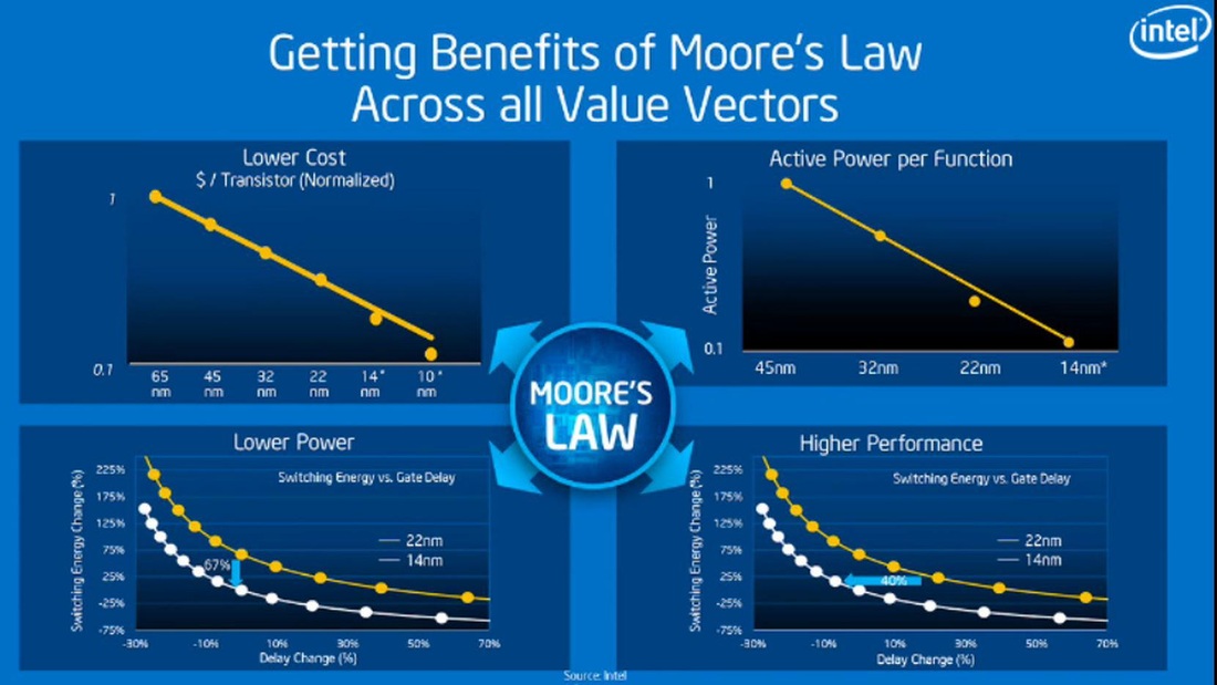
Figure 1
Maintaining dimensional scaling is in-line with Holt’s previous slide presented at the Jefferies May 2013 Analyst Meeting:
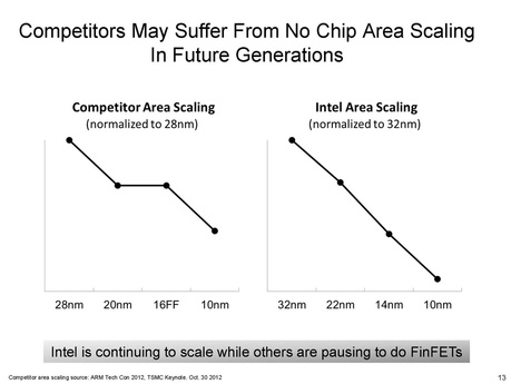
Figure 2
Here we observe the first discrepancy where Intel says they are "continuing to scale while others are pausing to do FinFETS”, while the other foundries say that their transistor cost will not be reduced for nodes below 28nm. This was made very clear by GlobalFoundries in it recent seminars and is nicely illustrated in this ASML Semicon West 2013 slide:
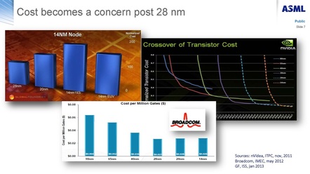
Figure 3
This has also been generally accepted by analysts. Below is a slide from IBS’s Handel Jones presentation at the CEA-LETI day in June of this year:
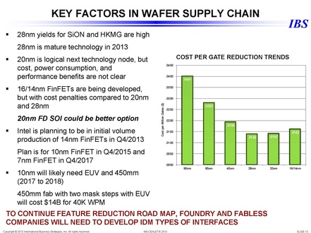
Figure 4
Some may argue that Intel will have a hard time competing as a foundry due to potential customer concern of Intel as a competitor. This is a valid point but it did not stop Apple to buy cell phone devices from Samsung.
Some may argue that Intel will have hard time competing due to the lack of broad EDA and IP support. This is also a valid point but Intel does not need to win all fabless designs. If Intel wins just the few super high volume designs, it may well win the war.
Some may argue that “Intel announced their high volume mobile SoFIA chips are mask fabricated at external foundry and do not use Intel internal manufacturing for at least next 2 years (2014-15). ALL of Intel's production for standalone modem chips today is outside Intel. Conclusion being Intel still does not have the right silicon technology for mobile computing which is why X86 less than 0.1% of Smartphone market" as one commenter at Intel Nears Foundry Inflection Point blog. This might be why Holt presented Intel’s plan to develop Foundry type processes. “Those products were optimized primarily for performance, and so Intel had avoided the problem that can crop up when transistors are packed more densely, namely that performance of the wires connecting transistors, the interconnects, can degrade. We didn’t scale the wires as much as we could have, because the products we were building didn’t demand that.” Now, he said, "the company’s technology would be focused more on those interconnects as Intel takes the scaling lead. The result would be the ability to more nimbly move between transistors optimized for performance, on the one hand, as in server and desktop chips, and transistors optimized for low-power mobile devices." as illustrated below:
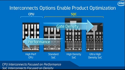
Figure 5
It would seem that if Intel could scale transistor cost as they have done in the last 40 years then they could win these super high volume consumer-oriented designs where cost is extremely important. And TSMC is clearly taking this seriously. As was made public after they lost Altera to Intel, TSMC aligned itself to face head-on Intel’s challenge by expediting the development of FinFet technology.
As TSMC's P/E is 14.42 while Intel's P/E is only 12.87 the market should have responded very well to these presentations but apparently it did not — and in reverse to NASDAQ trend, Intel stock fell more than 5% the day after:
As TSMC's P/E is 14.42 while Intel's P/E is only 12.87 the market should have responded very well to these presentations but apparently it did not — and in reverse to NASDAQ trend, Intel stock fell more than 5% the day after:
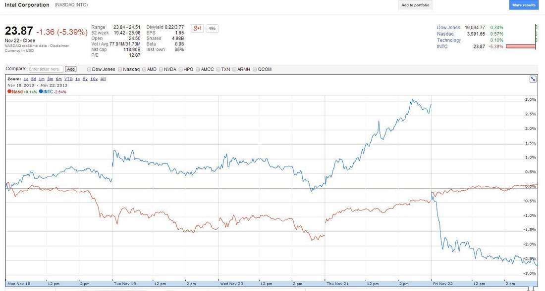
Figure 6
Nor did Altera's stock perform well since announcing the move to Intel as a foundry, especially when compared to Xilinx who choose to stay with TSMC, as the stock price chart below illustrates:
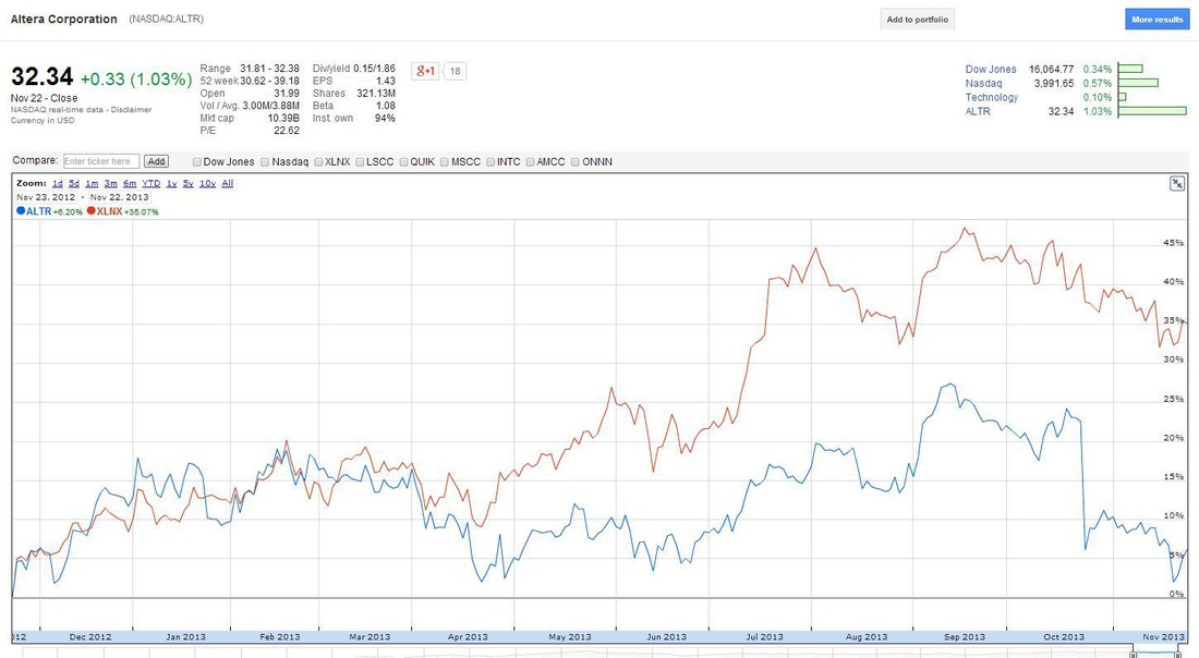
Figure 7
The Stock market might be wrong, as it been wrong many times before, but then there are other concerns:
There is one more important issue that seems to be ignored. For SoC applications the embedded SRAM is a key factor because it dominates the die area, as we recently presented in our blog Are we using Moore’s name in vain?. If Intel’s embedded SRAM is scaling each node as before then it would represent an important advantage over the foundries. Yet Intel recently announced integration of DRAM into Haswell and promised future Xeon and Xeon Phi models that integrate memory atop processors in 3D packages instead. Will these be aggressive enough to keep the on-system memory costs scaling?
- Why did Intel feel the need to put so much money in the ASML EUV program if they can do just as well without EUV?
- Does Intel reduced cost per transistor account for its escalating cost of R&D, which in 2013 averaged more than 20% of revenue vs. less than 14% in 2005?
- Does Intel reduced cost per transistor account for its escalating cost of capital, which, per their balance sheet on Depreciation/Depletion, averaged in 2013 more than 26% of revenue vs. less than 10% in 2011?
There is one more important issue that seems to be ignored. For SoC applications the embedded SRAM is a key factor because it dominates the die area, as we recently presented in our blog Are we using Moore’s name in vain?. If Intel’s embedded SRAM is scaling each node as before then it would represent an important advantage over the foundries. Yet Intel recently announced integration of DRAM into Haswell and promised future Xeon and Xeon Phi models that integrate memory atop processors in 3D packages instead. Will these be aggressive enough to keep the on-system memory costs scaling?

Figure 8
In short, if Intel could keep the traditional 30% cost reduction per node from 28nm to 10nm, and the foundry’s cost per transistor is staying flat, then Intel would be able to provide their foundry customers SoC products at a third of ther other foundries cost, and accordingly Intel should be able to do very well in its foundry business.


 RSS Feed