Monolithic 3D Inc., the Next Generation 3D-IC Company
  • Home
  • Technology
    • Technology
    • Papers, Presentations and Patents
    • Overview >
      • Background
      • Why Monolithic 3D?
      • Paths to Monolithic 3D
      • Applications
    • Ion-Cut: The Building Block
    • Monolithic 3D Logic >
      • RCAT
      • HKMG
      • Laser Annealing
      • RCJLT
      • 3D Embedded RAM
      • 3D Gate Array
      • FPGA
      • Ultra Large Integration - Redundancy and Repair
    • Monolithic 3D Memory >
      • 3D DRAM
      • 3D Resistive Memories
      • 3D Flash
    • Monolithic 3D Electro-Optics >
      • 3D Image Sensors
      • 3D Micro-Displays
  • 3D-IC Edge
    • 3D-IC Edge
  • News & Events
    • News & Events
    • S3S15 Game Change 2.0 Video/P
    • Webcast
    • Webinar
    • Press Releases
    • In the News
    • Upcoming Events
  • About Us
    • About Us
    • History
    • Team
    • Careers
    • Contact Us
  • Blog
  • Simulators

Can 450mm Decommoditize the Semiconductor Industry?

10/2/2011

7 Comments

 
Is the transition from 300mm to 450mm wafers just driven by 20-30% cost reduction? Or is there more to it than meets the eye? Let's take a look...

Picture
Figure 1: Intel, IBM, TSMC, Samsung and Globalfoundries are collaborating on 450mm research in New York.

Like many semiconductor enthusiasts, my day begins with a look at EETimes. Imagine my surprise a few days back when I saw a story about Intel, TSMC, IBM, Samsung and Globalfoundries joining forces to do 450mm chip R&D in New York (Figure 1)! Now, as we know, the 300mm to 450mm wafer transition can produce around 20-25% cost savings if all goes well. That raises the question: Are rivals such as Intel, TSMC and Samsung working together just to get 20-25% cost savings? Or is there more at stake?

Let's analyze the situation...

Figure 2 shows a plot of logic fab cost as a function of feature size. Does Figure 2 mean that a transition from 32nm to 22nm will cost companies $6.7B? No. Most tools from a 32nm logic fab can be reused for 22nm, and only a small percentage of new tools need to be bought. Companies such as Intel typically spend less than $2B when upgrading a single fab from 32nm to 22nm logic technology. (There are some exceptions to the rule, of course, but we'll talk about that in another blog post)

3d ic
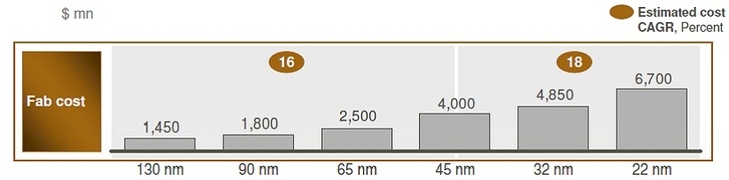
Figure 2: 300mm Logic Fab Cost as a Function of Feature Size (Courtesy: Globalfoundries)
A similar situation exists for memory. NAND flash memory makers, for example, used the same ASML 1900i immersion litho tools with double patterning for 3x nm and 2x nm and will possibly use the same tools for 1x nm. New tools were bought by NAND flash makers mainly when they built additional new fabs... upgrading existing fabs from 3x nm to 2x nm and now 1x nm allows one to reuse a lot of equipment. We know a 3x nm NAND flash fab costs $7B. A company doesn't pay $7B more when it scales this fab to 2x nm. It pays far less. And this makes scaling more palatable.

Moving to a different wafer size, such as 450mm, fundamentally breaks this model. When you move to a new wafer size, you need to upgrade ALL the equipment in your fab. This essentially means that you need to cough up $7B. You can't get away with paying just $2B. This requirement for large amounts of capital during wafer size transitions has caused many small players to exit the industry in the past. TSMC, in its paper titled Economic Analysis of 450mm Wafer Migration says, "The capital investment for larger wafer size fabs is increasing significantly, which creates an entry barrier to knock out weak players. For IC makers, about 130 companies had owned 150mm fabs. That number dropped to fewer than 90 for 200mm fabs and to about 24 for 300mm." It seems but natural to expect this trend to continue at 450mm.

A rule of thumb people use is that your revenue must be at least 2x greater than your fab cost to be able to afford it. To pay for a $7B 450mm fab, your revenue must therefore be at least $14B. Let's look at the different market segments in semiconductors and find out who can afford 450mm fabs.

3d ic
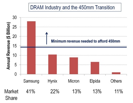
Figure 3: Total Semiconductor Revenue and DRAM Market Share for various Companies in 2010 (Source: EETimes)

In the DRAM business, only Samsung makes the cut, as Figure 3 indicates. All other DRAM makers, who together make up 60% of the DRAM market, may be unable to afford the 450mm transition. Their costs are therefore going to be ~25% more than Samsung, which is quite significant for DRAM. Not just that, equipment makers are not expected to support scaling on 300mm after the transition to 450mm. For example, no immersion litho tools are available for 200mm wafers now that the transition to 300mm has occured. This prevents 200mm manufacturers from scaling to small feature sizes. Due to the above reasons, a DRAM manufacturer who doesn't move to 450mm may eventually have to exit the business.

3d ic
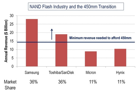
Figure 4: Total Semiconductor Revenue and NAND Flash Market Share for various Companies in 2010 (Source: EETimes)

In the NAND flash memory business, only Samsung and Toshiba/SanDisk may be able to afford 450mm fabs (Figure 4). All other manufacturers, who together make up 28% of the flash market, may be unable to afford 450mm and may eventually be forced to exit. Expect to see many of the smaller players in DRAM and NAND flash try and get national governments to pay for 450mm fabs to stay relevant. Also expect to see more alliances between manufacturers...

3d ic
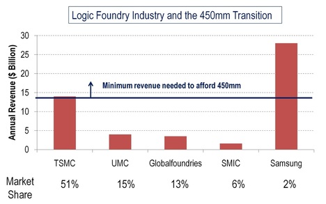
Figure 5: Total Semiconductor Revenue and Logic Foundry Market Share for various Companies in 2010 (Source: EETimes)

In the foundry business, only TSMC and possibly Samsung can afford a 450mm fab, as Figure 5 shows. Globalfoundries, as we know, is lucky enough to be sponsored by the Government of Abu Dhabi, who could potentially get them a 450mm fab. The other foundry players, who make up 36% of today's foundry market, may be unable to afford a 450mm fab :-( Foundries who cannot afford 450mm may need to remodel themselves as analog/RF/trailing-edge node suppliers.

How would this new world with possibly one low-cost DRAM producer, two low-cost NAND producers and two or three low-cost foundries look? Well, in this new world, semiconductor products would no longer be commodities. Yes, even memory products such as DRAM and NAND flash could become decommoditized. Let me explain why... Memory prices are determined by how competitive the market is. In a world with just one or two competitive memory manufacturers, it is possible that these manufacturers could boost their profit margins quite significantly. Needless to say, logic manufacturers would reap significant benefits from having less competition too.

The 450mm transition hasn't found much favor with equipment makers yet, since it doesn't exactly increase their market. Some equipment makers say 450mm may never happen. But expect Intel, Samsung and TSMC to push aggressively for it. And they'll push for it not just because it reduces costs by 20-25%... they'll push for it also because it helps them force out competitors and boost profit margins. In fact, one of the biggest proponents for 450mm seems to be Morris Chang of TSMC. The old warhorse, who is considered the Andy Grove of our times, has no doubt seen what I'm describing to you above. A decommoditized semiconductor business would be wonderful, wouldn't it? At least for the ones left standing at the end of it all...
Picture
- Post by Deepak Sekar
7 Comments
george storm
10/3/2011 07:36:56 pm

Few can disagree that 450-mm will support the trend towards consolidation.

Indeed, unless equipment suppliers find it worth continuing to manufacture leading-edge equipment for 300mm FABs, it does indeed look as if the foundry business will become concentrated in at most three or four companies at geometries of 22-nm and below (the number will probably be set by 'political' views on security of supply, rather than by pure economics).

However, I doubt that this effect alone will 'decommoditize' memory. Firstly, it would seem that at least Hynix and Micron could overcome the hurdle by producing DRAM and Flash in the same fabs. Second, if companies had applied this multiplier in the past, foundries like UMC, Global, and SMIC would still be limited to 200mm wafers.

I suspect that part of the reason for the discrepancy between this theory and companies' practice is that the quoted factor may be the level at which it is worth building a new FAB and mothballing the old, rather than the level at which the new FAB can be profitable. I.e. it is not the level of affordability, but the level at which the switch would be desirable for geometries that can still be produced in smaller-diameter fabs.

An additional factor for memory would be the anticipated growth in NV product with the increasing penetration of SSDs.

Reply
Deepak Sekar
10/3/2011 09:46:33 pm

@George:

Good points.

If we end up in a scenario with just 1-2 memory manufacturers, I feel it will indeed cease being a commodity. There are a number of ways to tackle this issue for the second tier manufacturers - such as building a 450mm fab in a country where the Government pays for it, or by forming collaborations like I've listed in the blog post... but both of these are high-risk avenues. Keep in mind that some second tier memory manufacturers have serious issues with cash flow even today.

The first 300mm foundry fabs were in nodes were fabs were not as costly... so they were easier to afford.

Reply
Bob Merritt link
10/5/2011 07:45:12 am

Great article. However one comment would be that it appears your assumption relative to memory technologies is that the system-level performance contribution of memory continues to be related primarily to the cost per bit as a data storage device and with little opportunity for other higher-level value attributes. Such a model is of course epitomized by industry-standard DRAMs in periods during the rapid growth of desktop PCs.

We have advised our clients to consider a different role for the future evolution of memory technologies in which a wider range of performance attributes leads to a higher valued and much less commoditized market environment for memory products. Elements that would support this scenario are already visible in the increasing demand for non-volatile memory technologies supporting the trend toward high-performance mobile applications, the balancing of cost-per-bit versus power consumption in the usage of SSDs versus DRAMs in enterprise applications, and the ongoing market experimentation with the limits of NAND memory cell endurance versus the cost-per-bit of NAND.

Factor into that scenario the impact of multi-die hybrid packages capable of providing sub-system levels of performance as envisioned by the more recent system-in-package ITRS projections--which we believe expands the range of memory performance attributes to an even broader array of value points.

In this alternate scenario, the commodity aspect of memory technologies continues to decrease in significance anyway due to increased requirements for a broader range of memory cost/performance tradeoffs. Therefore the 450mm impact we expect to see on the memory technologies is that the demand for commodity-like memory products will shift to the 450mm processes as you suggest, while the increasing value of memory products with a broader range of performance attributes will continue to be cost effectively supported on 300mm fabs. Under our scenario, the memory market does not automatically and immediately consolidate around only those suppliers able to afford 450mm fabs, with the cost effectiveness of the mature 300mm equipment being extended by the introduction of new and emerging memory technologies.

Reply
Steve L
10/11/2011 07:57:58 am

450mm brings the semi front end manufacturing world into the mature business line category. As such, then business strategies such as the "Rule of 3" come into play and the motivation of a companies strategy shifts from market share to profit. There are plenty of markets that operate transacting commodities but make gobs of money for example the Oil and Gas industries.

So I'd recommend backing up to the headline business strategy and work down given a fundamental consolidation of how access to the most cost efficient form of manufacturing (450mm) will force structural changes in the market participants. It literally will come down to are who is a Generalist or a Specialist, those in the middle will get killed. But I really don't see the whether the product is a commodity or not has much bearing on this outcome.

Reply
Donald P Hutchins
11/8/2011 02:13:30 pm

I had this idea 25 years ago, somebody must have actually listened, I figured out the topology and optical paths, heat removal, power factors, and the whole nine yards, for a 2" cube, that would do 50 teraflops/sec and consume maybe 35 watts, with parallel address and data paths, that could be easily configured for just about any job.

Reply
jobs in ghana link
6/26/2012 04:49:15 pm

Thank u for post, its nice and I gone through full post, interesting. Keep posting....

Reply
resumesplanet reviews link
10/3/2012 07:37:12 pm

Can 450mm Decommoditize the Semiconductor Industry? thank you for answering this question of mine as it is raising from many days..Thank you for such a fantastic blog. Where else could anyone get that kind of info written in such a perfect way? I have a presentation that I am presently working on, and I have been on the look out for such information.

Reply

Your comment will be posted after it is approved.


Leave a Reply.

    Search Blog


    Meet the Bloggers


    Follow us


    To get email updates subscribe here:


    Recommended Links

    3D IC Community
    3D IC LinkedIn Discussion Group

    Recommended Blogs

    • 3D InCites by Francoise von Trapp
    • EDA360 Insider by Steve Leibson
    • Insights From the Leading Edge by Phil Garrou
    • SemiWiki by Daniel Nenni, Paul Mc Lellan, et al.

    Archives

    March 2022
    December 2021
    August 2021
    August 2018
    July 2018
    May 2018
    October 2017
    September 2017
    December 2016
    September 2016
    August 2016
    November 2015
    October 2015
    September 2015
    July 2015
    June 2015
    May 2015
    April 2015
    March 2015
    February 2015
    October 2014
    September 2014
    August 2014
    July 2014
    June 2014
    May 2014
    April 2014
    March 2014
    February 2014
    January 2014
    December 2013
    November 2013
    October 2013
    September 2013
    August 2013
    July 2013
    March 2013
    February 2013
    January 2013
    December 2012
    November 2012
    October 2012
    August 2012
    June 2012
    May 2012
    April 2012
    March 2012
    February 2012
    January 2012
    December 2011
    November 2011
    October 2011
    September 2011
    August 2011
    July 2011
    June 2011
    May 2011
    April 2011
    March 2011

    Categories

    All
    3d Design And Cad
    3dic
    3d Ic
    3d Nand
    3d Stacking
    3d Technology
    Brian Cronquist
    Dean Stevens
    Deepak Sekar
    Dram
    Education
    Heat Removal And Power Delivery
    Industry News
    Israel Beinglass
    Iulia Morariu
    Iulia Tomut
    Monolithic3d
    Monolithic 3d
    MonolithIC 3D Inc.
    Monolithic 3d Inc.
    Monolithic 3d Technology
    Moore Law
    Outsourcing
    Paul Lim
    Repair
    Sandisk
    Semiconductor
    Semiconductor Business
    Tsv
    Zeev Wurman
    Zvi Or Bach
    Zvi Or-Bach

    RSS Feed

© Copyright MonolithIC 3D Inc. , the Next-Generation 3D-IC Company, 2012 - All Rights Reserved, Patents Pending