A few weeks back, in my "Looking Beyond Lithography" post, I explained the reasons why flash memory makers such as Toshiba, Samsung and Hynix are exploring an alternative approach to Moore's law. In this blog-post, let's see if this approach is viable for logic technologies...
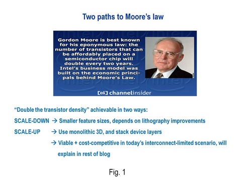
All of us are familiar with Moore's law: "The number of components on a chip doubles every 2-3 years". Most people interpret this as a feature-size reduction issue. Meaning that every 2-3 years, you reduce transistor and interconnect feature sizes by 0.7x and area by 0.5x, so you double the number of components on a chip. This approach, as many of you know, is referred to as "SCALE DOWN" in our industry. But there is another approach to Moore's law, and it is getting increasing attention. We call it "SCALE UP". Essentially, you can double the number of components on a chip by using monolithic 3D technology and doubling the number of stacked device layers. In today's interconnect-limited scenario, this alternative approach to Moore's law is economically viable for logic technologies and can give the performance/power benefits consumers are used to. Let me show you the math...
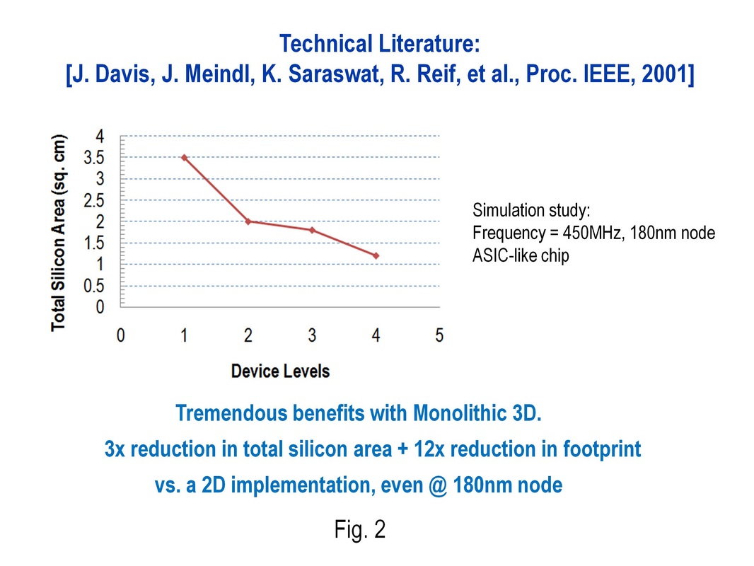
We know that for conventional feature-size scaling (SCALE DOWN), the die size of a logic core reduces by 0.5x and power reduces by 0.5x when it is ported "as-is" to the next technology node. It raises the question, "For SCALE UP, what are the corresponding numbers?" Well, a number of publications have explored this question. Davis, Meindl, Reif, Saraswat, et al. reported a 3x reduction in die size for a certain target performance at the 180nm node, as shown in Fig. 2. They mention that with monolithic 3D, average wire lengths reduce. The gates that drive these wires can then be made smaller in size. They suggest that both these factors result in reduced die size, which in turn reduces wire lengths further. Zhou, et al. did the lay-out of a Low-Density Parity Check (LDPC) decoder in 3D, and showed significant benefits as well (Fig. 3).

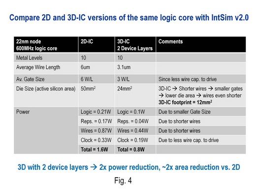
In our company, we did a study to estimate the benefits of monolithic 3D for a leading-edge 22nm technology. We used IntSim v2.0, an open-source CAD tool I described in my last blog-post. You'll see a summary of results with IntSim v2.0 in Fig. 4. Monolithic 3D's reduced interconnect lengths enable a gate size reduction, which in turn reduces die size and power significantly. Overall, one gets a 2x reduction in die size and 2x reduction in power when doubling the number of stacked device layers. The numbers for SCALE UP are comparable to the ones for SCALE DOWN in today's interconnect-limited scenario! Note that to get the large benefits shown in Fig. 2, Fig. 3 and Fig. 4, it is important to have vertical connection sizes comparable to horizontal connection sizes (in the tens of nm range). This allows true three-dimensional circuits.
Now that I've told you about the power, performance and area implications of monolithic 3D, let's discuss die cost. We have a Cost-Of-Ownership spreadsheet in our company which estimates the wafer cost of a leading-edge 22nm technology based on the process steps used. This spreadsheet was prepared in accordance with the Sematech Cost-Of-Ownership methodology (Israel Beinglass, Usha Raghuram and Zvi Or-Bach gave me many useful inputs and suggestions while preparing this spreadsheet, thank you Israel, Usha and Zvi!). Well, we used this calculator to obtain the numbers in Fig. 5 and Fig. 6. The key points to note are:
- For SCALE UP, you can use depreciated equipment when you double the number of device layers. Essentially, you can use your fab equipment for a 22nm 2D technology for 2 years, and then use the same equipment for 2 more years on a 22nm 3D technology! Since the equipment cost halves due to depreciation every 2 years, this is a key advantage. Let's say, for example, you bought a set of immersion litho tools for your 22nm process at a cost of $42M each in 2011. If you need to go to 15nm technology in 2013, you might need to pay up $100M each for a set of EUV tools. On the other hand, if you moved to a 22nm 3D technology in 2013, the cost of a litho tool is $21M, since the immersion tools have depreciated 50% in value the past 2 years.
- For doubling the number of stacked device layers, the amount of additional equipment required is not much, and could cost less than $100M (Fig. 6). On the other hand, a shift to a smaller feature size requires changes to (costly) lithography tools and a whole bunch of other stuff and could cost anywhere between $1.1B and $4B. In today's scenario, when fabs are becoming unaffordable for most people, this is a key consideration.


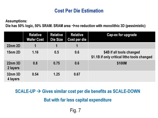
While I showed you die size reduction numbers for logic cores in Fig. 4, SRAM does not benefit in similar ways (there are some creative ways of using monolithic 3D for caches that can give much benefit, but we'll not consider those in this analysis). Since SRAMs can take up as much as 50% of a logic chip's die area, this needs to be considered. Due to this, the overall die size reduction numbers for the (logic core + SRAM) combination are not as good for monolithic 3D as conventional feature-size scaling. Fig. 7 shows though, that even with this considered, SCALE UP can give similar cost per die compared to SCALE DOWN, largely due to the use of depreciated equipment.
What's the bottom line?
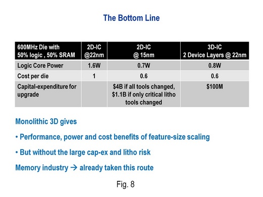
A summary of our analysis is shown in Fig. 8. It can be observed that SCALE UP can provide power and cost per die benefits similar to SCALE DOWN, but requires significantly lower capital expenditure. This is particularly relevant today as fabs are becoming unaffordable for most semiconductor manufacturers. Furthermore, litho tool costs and risks are increasing exponentially, making attractive an alternative to Moore's law that doesn't rely on litho improvement. The flash memory industry, which scales faster than the logic industry, has hit these issues already, and is actively exploring SCALE UP. Will the logic industry follow suit? We think yes...
A summary of our analysis is shown in Fig. 8. It can be observed that SCALE UP can provide power and cost per die benefits similar to SCALE DOWN, but requires significantly lower capital expenditure. This is particularly relevant today as fabs are becoming unaffordable for most semiconductor manufacturers. Furthermore, litho tool costs and risks are increasing exponentially, making attractive an alternative to Moore's law that doesn't rely on litho improvement. The flash memory industry, which scales faster than the logic industry, has hit these issues already, and is actively exploring SCALE UP. Will the logic industry follow suit? We think yes...


 RSS Feed