We can still make transistors smaller but not cheaper

We have a guest contribution from Zvi Or-Bach, the President and CEO of MonolithIC 3D Inc. Mr. Or-Bach discusses about the fact that Moore's Law at 28nm.
We have been hearing about the imminent demise of Moore’s Law quite often recently. Most of those predictions have been targeting the 7nm node and 2020 as the end point. But we need to recognize that 28nm is actually the last node of Moore's Law, beyond which we can make smaller transistors and pack more of them into the same die size but we can not reduce the cost, and in most cases, the same SoC will have a higher cost!
The famous Moore's Law was presented as an observation by Moore in his 1965 Electronics paper "The future of integrated electronics". Quoting: "The complexity for minimum component costs has increased at a rate of roughly a factor of two per year. Certainly over the short term this rate can be expected to continue, if not to increase. Over the longer term, the rate of increase is a bit more uncertain, although there is no reason to believe it will not remain nearly constant for at least 10 years." Clearly Moore's Law is about "The complexity for minimum component costs", and the minimum component cost will be at the 28nm node for many years, as we will detail in the remainder of this blog.
The following chart was presented by ST’s Joël Hartmann (EVP of Manufacturing and Process R&D, Embedded Processing Solutions) during Semi’s recent ISS 2014 Europe Symposium:
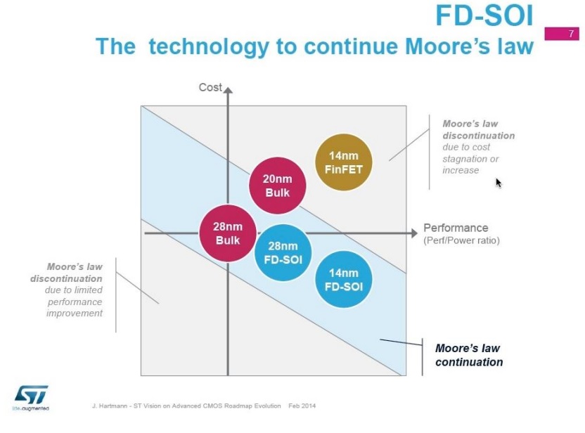
Hartmann is making the case that the "Moore's Law discontinuation due to cost stagnation or increase" applies to bulk technologies, which is the technology base of the majority of the industry.
ST information is backed by Globalfoundries as we can see from the following chart presented at the 2013 SOI Consortium workshop in Kyoto, Japan.
ST information is backed by Globalfoundries as we can see from the following chart presented at the 2013 SOI Consortium workshop in Kyoto, Japan.
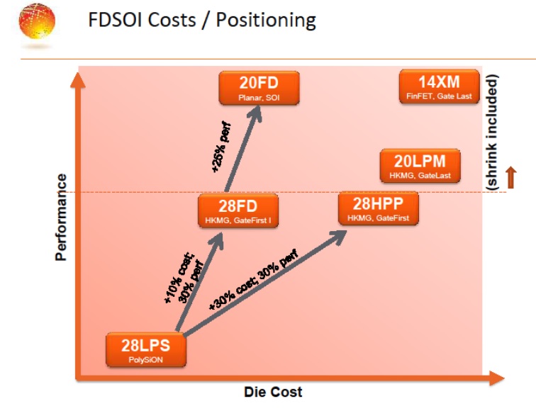
The above Globalfoundries chart shows that the lowest cost transistor is at the polySiON 28nm node.
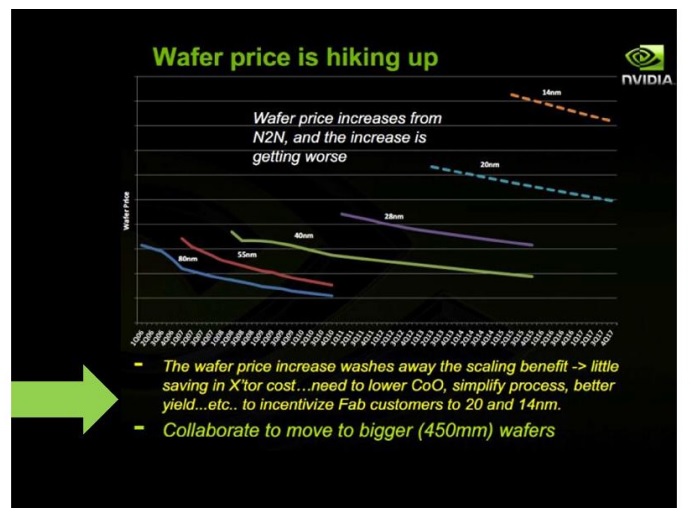
Beyond 28nm, scaling becomes extremely expensive due to double litho, HKMG, FinFET, etc. The increase in wafer cost is illustrated by the recent NVidia chart from Semicon Japan (Dec. 2013) below:
Beyond 28nm, scaling becomes extremely expensive due to double litho, HKMG, FinFET, etc. The increase in wafer cost is illustrated by the recent NVidia chart from Semicon Japan (Dec. 2013) below:
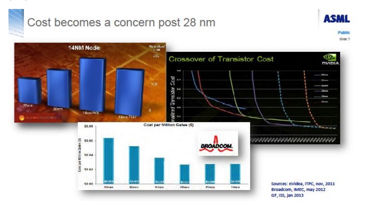
The increase in wafer cost eats away the 2X transistor density gain per node as is illustrated by this ASML slide from Semicon West (2013):
However, the SoC end product silicon area is dependent on the SRAM bit cell size far more than on the general transistor density. This is the fundamental challenge now facing dimensional scaling - SRAM Bit scaling has been dramatically slowed beyond 28nm.
At 28nm the bitcell size is about 0.12µm². The following chart by imec reported in Status update on logic and memory roadmaps (Oct 2013):
At 28nm the bitcell size is about 0.12µm². The following chart by imec reported in Status update on logic and memory roadmaps (Oct 2013):
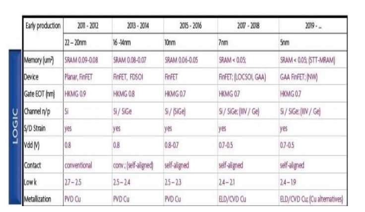
Beyond 28nm, the SRAM bit scaling rate is about 20% per node instead of the historical 50%. And the situation is actually far worse as is illustrated by the following chart, presented in an invited paper by Dinesh Maheshwari, CTO of Memory Products Division at Cypress Semiconductors, at ISSCC 2014. It was also at the center of our recent blog "Embedded SRAM Scaling is Broken and with it Moore's Law."
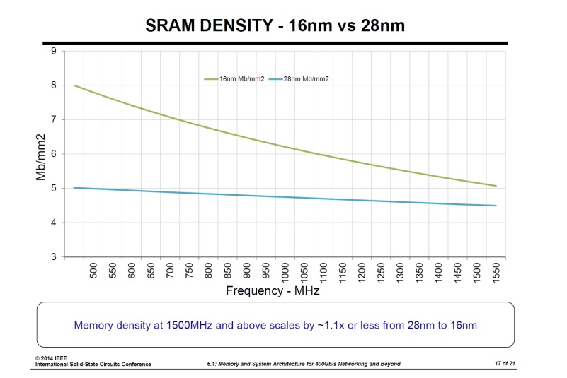
Accordingly, the SRAM Mb/mm² scales far less than the bitcell due to factors such as:
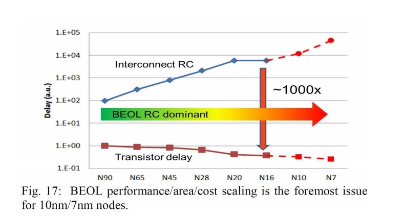
Furthermore, the exponential increase in BEOL RC as is illustrated by the following chart, presented by Geoffrey Yeap, VP of Technology at Qualcomm in his invited IEDM 2013 paper, results in an exponential increase of number of drivers and repeaters. This suppresses the effective gate density increase to only a factor of x1.6, or less.
- Smaller transistors have less drive, thus requiring breaking the SRAM into smaller blocks, creating more overhead area costs
- Smaller transistors have a higher level of variation, also requiring breaking the SRAM into smaller blocks
- The need for more overhead such as read assist circuits and write assist circuits
- Tighter metal pitches begat higher RC, thus again requiring breaking the SRAM into smaller blocks
Furthermore, the exponential increase in BEOL RC as is illustrated by the following chart, presented by Geoffrey Yeap, VP of Technology at Qualcomm in his invited IEDM 2013 paper, results in an exponential increase of number of drivers and repeaters. This suppresses the effective gate density increase to only a factor of x1.6, or less.
Summarizing all of these factors, it is clear that for most SoCs, the 28nm will be for the coming years the node for "minimum component costs".
As an industry, we are facing a paradigm shift because dimensional scaling is no longer the path for cost scaling. New paths need to be explored such as SOI and monolithic 3D integration. It is therefore fitting that the traditional IEEE conference on SOI has expanded its scope and renamed itself to IEEE S3S: SOI technology, 3D Integration, and Subthreshold Microelectronics. The 2014 S3S conference is scheduled for October 6-9, 2014 at the Westin San Francisco Airport. This new unified conference will help us to improve efficiency and establish this conference as a world class international venue to present and learn about the most up-to-date trends in CMOS and post-CMOS Scaling. The conference will provide both educational and cutting edge research in SOI and monolithic 3D and other supporting domains. These technologies were not part of the mainstream semiconductor past; accordingly, it is a golden opportunity to catch-up with these technologies now. Please mark your calendar for this opportunity to contribute and learn about SOI and monolithic 3D technology, as these technologies are well positioned to keep the semiconductor industry's future momentum.
As an industry, we are facing a paradigm shift because dimensional scaling is no longer the path for cost scaling. New paths need to be explored such as SOI and monolithic 3D integration. It is therefore fitting that the traditional IEEE conference on SOI has expanded its scope and renamed itself to IEEE S3S: SOI technology, 3D Integration, and Subthreshold Microelectronics. The 2014 S3S conference is scheduled for October 6-9, 2014 at the Westin San Francisco Airport. This new unified conference will help us to improve efficiency and establish this conference as a world class international venue to present and learn about the most up-to-date trends in CMOS and post-CMOS Scaling. The conference will provide both educational and cutting edge research in SOI and monolithic 3D and other supporting domains. These technologies were not part of the mainstream semiconductor past; accordingly, it is a golden opportunity to catch-up with these technologies now. Please mark your calendar for this opportunity to contribute and learn about SOI and monolithic 3D technology, as these technologies are well positioned to keep the semiconductor industry's future momentum.


 RSS Feed