Beyond the Clouds: Edge-to-Edge Transformation
"Welcome to another episode of "Beyond the Clouds: Edge-to-edge Transformation." Today, we have the privilege of speaking with Zvi Or-Bach, founder and CEO of MonolithIC 3D. Zvi's journey in the semiconductor industry is a fascinating tale of innovation, risk-taking, and relentless pursuit of technological advancement.
Zvi Or-Bach's roots trace back to Israel, where his early academic pursuits at Technion laid a strong foundation for his future endeavors. After completing his bachelor's degree in engineering, he served as a technical officer in the Israeli army. This unique blend of military discipline and academic excellence continued at the Weizmann Institute, where he earned a master's degree in Computer Science. It was during this period that Zvi's work on real-time video imaging caught the attention of Honeywell, leading to his first foray into the American tech landscape.
At Honeywell, Zvi immersed himself in the vibrant startup culture of the 128 Corridor, the second hub of innovation after Silicon Valley. His entrepreneurial spirit was further ignited when he returned to Israel as a chief engineer at Elbit Computers. This role not only bolstered his credentials but also set the stage for his first major entrepreneurial venture—Cubic Space Chips.
Chip Express marked Zvi's transition from a promising engineer to a visionary entrepreneur. The company initially aimed to sell laser micro-machining devices but pivoted to providing rapid prototyping services, a move that resonated with the burgeoning tech scene in Silicon Valley. Their innovative approach quickly attracted major clients, including Apple, and established Chip Express as a significant player in the industry.
Zvi's next venture, eASIC, came during the dot-com boom. Despite the initial challenges and the eventual sale to Intel, eASIC was instrumental in pioneering Structured ASIC technology, demonstrating Zvi's ability to stay ahead of industry trends. His resilience during the dot-com bust, funding operations out of his own pocket, showcased his unwavering commitment to innovation.
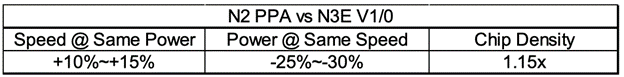
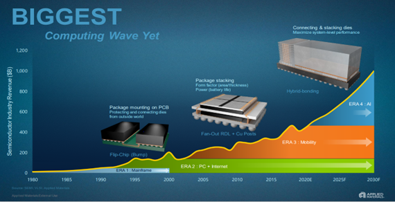
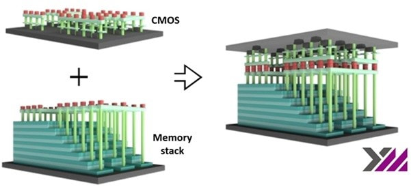
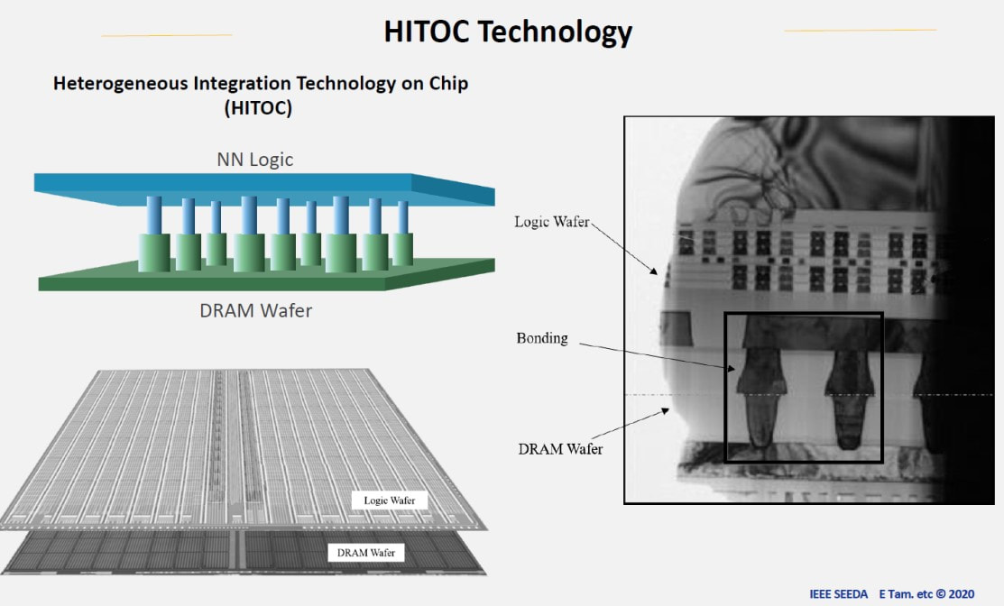
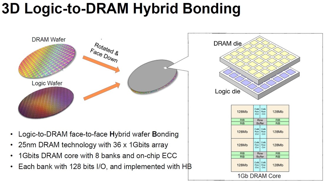
MonolithIC 3D, Zvi's current endeavor, epitomizes his vision for the future of semiconductors. Recognizing the limitations of traditional 2D scaling, Zvi has championed the shift towards 3D integration. His company's breakthroughs in hybrid bonding technology promise to revolutionize the industry by enabling higher performance and lower costs. Despite the initial skepticism, Zvi's persistence has paid off, with major industry players like AMD and Micron now adopting hybrid bonding.
Throughout his career, Zvi has been driven by a fearless attitude towards risk. His belief in the importance of innovation over complacency has been a guiding principle, one that he advises aspiring entrepreneurs to embrace. The path to success, according to Zvi, is fraught with challenges, but the potential rewards make the journey worthwhile.
In addition to his professional achievements, Zvi's contributions extend to mentoring and supporting other startups. His role as chairman of Zeno Semiconductors and his ongoing efforts to develop new innovations reflect his dedication to nurturing the next generation of tech leaders."
Zvi Or-Bach's roots trace back to Israel, where his early academic pursuits at Technion laid a strong foundation for his future endeavors. After completing his bachelor's degree in engineering, he served as a technical officer in the Israeli army. This unique blend of military discipline and academic excellence continued at the Weizmann Institute, where he earned a master's degree in Computer Science. It was during this period that Zvi's work on real-time video imaging caught the attention of Honeywell, leading to his first foray into the American tech landscape.
At Honeywell, Zvi immersed himself in the vibrant startup culture of the 128 Corridor, the second hub of innovation after Silicon Valley. His entrepreneurial spirit was further ignited when he returned to Israel as a chief engineer at Elbit Computers. This role not only bolstered his credentials but also set the stage for his first major entrepreneurial venture—Cubic Space Chips.
Chip Express marked Zvi's transition from a promising engineer to a visionary entrepreneur. The company initially aimed to sell laser micro-machining devices but pivoted to providing rapid prototyping services, a move that resonated with the burgeoning tech scene in Silicon Valley. Their innovative approach quickly attracted major clients, including Apple, and established Chip Express as a significant player in the industry.
Zvi's next venture, eASIC, came during the dot-com boom. Despite the initial challenges and the eventual sale to Intel, eASIC was instrumental in pioneering Structured ASIC technology, demonstrating Zvi's ability to stay ahead of industry trends. His resilience during the dot-com bust, funding operations out of his own pocket, showcased his unwavering commitment to innovation.
MonolithIC 3D, Zvi's current endeavor, epitomizes his vision for the future of semiconductors. Recognizing the limitations of traditional 2D scaling, Zvi has championed the shift towards 3D integration. His company's breakthroughs in hybrid bonding technology promise to revolutionize the industry by enabling higher performance and lower costs. Despite the initial skepticism, Zvi's persistence has paid off, with major industry players like AMD and Micron now adopting hybrid bonding.
Throughout his career, Zvi has been driven by a fearless attitude towards risk. His belief in the importance of innovation over complacency has been a guiding principle, one that he advises aspiring entrepreneurs to embrace. The path to success, according to Zvi, is fraught with challenges, but the potential rewards make the journey worthwhile.
In addition to his professional achievements, Zvi's contributions extend to mentoring and supporting other startups. His role as chairman of Zeno Semiconductors and his ongoing efforts to develop new innovations reflect his dedication to nurturing the next generation of tech leaders."


 RSS Feed