In today's blog post, we'll look at the Xilinx 2.5D FPGA and analyze its pros and cons...
The Xilinx 2.5D FPGA has met with widespread acclaim since its launch in October 2010. EETimes called it "the world's highest capacity FPGA". Two of my favorite bloggers, Steve Leibson and Francoise von Trapp, had positive things to say about it too. Steve dubbed it "generation-jumping" and Francoise said "it has got the 3D IC market segment abuzz". Since I specialize in this field, people frequently ask me about pros and cons of 2.5D FPGAs, and want to know if the press attention is justified. Thought I should write a blog-post on the subject today.
The Xilinx 2.5D FPGA Technology
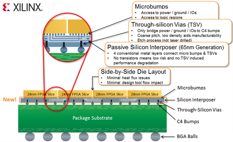
Figure 1: The Xilinx 2.5D FPGA Product.
Like all semiconductor chips, FPGAs face issues getting good yields for large dice. The 2.5D idea addresses this problem. Large 1.9M gate FPGAs are built using four smaller FPGA dice atop a silicon interposer that offers a high density of connections. As you can imagine, the smaller FPGA dice are much easier to yield. They are built with a 28nm process while the silicon interposer is built with a 65nm process utilizing four conventional metal layers, microbumps and through-silicon vias. 10k-30k connections run between FPGA dice on the interposer.
With this technology, Xilinx claims it can offer 2x more gates compared to conventional FPGAs.
Why Silicon Interposers?
For the 2.5D FPGA application, a high density of inter-chip connections is required, which is not possible with conventional organic packages. This is for multiple reasons:
- The co-efficient of thermal expansion (CTE) mismatch between silicon dice (3ppm/K) and organic substrates (18ppm/K) is large. Due to this, severe reliability issues arise and prevent use of small high-density solder bumps. The CTE of a silicon interposer is the same as the chip, so a high density of I/O connections can be formed. For example, Xilinx's 2.5D FPGA has 45um pitch microbumps compared to ~100um pitch I/O used for organic substrates. Underfill need not be used for silicon interposers. Package-level stresses are therefore not communicated to low k dielectrics on the chip, improving their mechanical integrity.
- Due to their smoothness and dimensional stability, silicon interposers allow small line widths to be printed on them. In addition, the infrastructure and depreciated tools available for chip processing can produce silicon interposers. Line widths on silicon interposers are below 1um, compared to 20um for organic substrates.
- Capture more of the ASIC market: FPGAs have many advantages over ASICs, such as lower Non-Recurring Engineering (NRE) costs, shorter time-to-market, field programmability and easier scalability. Despite this, the FPGA market is quite small, and forms only around 15%-20% of the total ASIC market. This is largely because FPGAs have ~20-40x lower density, ~10x higher power and ~3x lower performance compared to ASICs at the same node. The 2x higher gate count with silicon interposers enables Xilinx to address more of the ASIC market.
- Future trend - DRAM on the interposer: Although the Xilinx product just had logic chips on the interposer, many believe DRAM on the interposer could happen soon. See Fig.2. This could boost FPGA performance dramatically due to the higher memory access speeds.
- Future trend - SERDES on the interposer: Instead of integrating SERDES transceivers, Xilinx talks about using a separate SERDES die on the interposer in the future (Fig. 2). By utilizing a high performance process technology for SERDES blocks and a low power process technology for logic blocks, significant benefits can be obtained.

Figure 2: DRAM and SERDES die could be placed on the silicon interposer in the future.
- Future trend - Affordable product families: As you'd know, today's FPGAs are SoCs consisting of Logic Cells, Transceivers, Block RAM, DSPs, etc. Different customers require varying amounts of these building blocks. For example, at the 28nm node, Xilinx sells 27 products having different logic cell, transceiver, block RAM and DSP slice counts. Considering the high costs associated with masks and inventory, it is expensive to build product families this way. Here's an alternative approach I heard from Zvi Or-Bach, MonolithIC 3D Inc.'s CEO. Let's say you build 4 chip types: Chip 1 = 'w' logic cells, Chip 2 = 'x' transceivers, Chip 3 = 'y' DSP slices, Chip 4 = 'z' block RAM cells. You can create products with various combinations and multiples of Chips 1-4 on a silicon interposer, without needing new mask sets. Of course, this requires interposer costs to be low.
- Future trend - Has the potential to disrupt the IP industry: A SoC today includes many IP blocks, whose RTL code the SoC designer combines. If 2.5D gets cheap enough someday, IP blocks could be manufactured as separate dice and assembled together on an interposer. Each of these IP blocks could benefit from economies of scale. New paradigms may emerge. For example, a 130nm node analog IP block could be combined with a 32nm node ARM core. IP blocks can be reused effectively as well. IP suppliers will need to make radical changes to their business model if this happens - they will be manufacturing hardware instead of providing RTL code. We've often heard predictions about the demise of the ASIC industry. Could this be the new ASIC? (Caveat: Silicon interposer costs need to reduce dramatically for this to happen!)
Cost
The idea of using silicon interposers is not new. Many companies sold silicon interposer products in the 1990s. This includes companies such as Micro Module Systems (a DEC spin-off), nChip and others. In fact, Zvi Or-Bach, our company's CEO, says he visited Micro Module Systems in the early 1990s and saw their silicon interposer fab! See Figure 3 for pictures of some silicon interposer products. Unfortunately, the technology did not work out due to cost issues.
The idea of using silicon interposers is not new. Many companies sold silicon interposer products in the 1990s. This includes companies such as Micro Module Systems (a DEC spin-off), nChip and others. In fact, Zvi Or-Bach, our company's CEO, says he visited Micro Module Systems in the early 1990s and saw their silicon interposer fab! See Figure 3 for pictures of some silicon interposer products. Unfortunately, the technology did not work out due to cost issues.
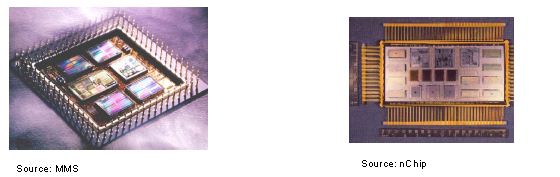
Figure 3: Silicon interposer products from the 1990s.
Is cost still an issue? Hmmm, it could be. SemiMD and Ultratech say a 300mm 65nm interposer wafer costs $10,000, which is several times larger than the cost of a 28nm high-k/metal gate wafer! The high cost is apparently because economies of scale haven't kicked in, and few interposer suppliers exist. Its not surprising that Xilinx is targeting the 2.5D FPGA towards cost-insensitive applications, such as ASIC prototyping, military equipment as well as high-end computing and communications.
The next question to ask is: will cost go down when economies of scale kick in? Yole Developpement, an analyst firm, claims interposers built with depreciated 300mm equipment could cost as low as $615 per wafer. They mention this is below the $700 per wafer (1 cent per sq. mm) required for large scale adoption. Another analysis on interposer cost from eSilicon reached similar conclusions.
A number of ideas to tackle the cost problem are emerging. A stealth mode subsidiary of Cypress called Deca Technologies claims it is developing a method to dramatically reduce the cost of silicon interposers (see this article from Steve Leibson). Another approach to lowering cost is from Georgia Tech, which uses glass interposers. Glass provides much of the technical benefits of silicon. More importantly, it allows one to use the large panel sizes and infrastructure of the LCD industry to lower cost. In terms of Xilinx's cost reduction plan, the company believes 3D will be the next step after 2.5D. See Fig. 4. By stacking chips atop each other instead of placing them side-by-side, the area required for the silicon interposer is reduced, thereby lowering the cost.
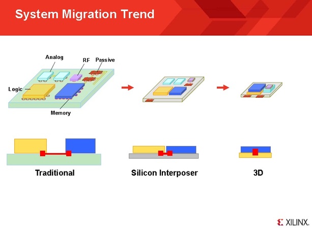
Figure 4: Xilinx feels 3D will be the next step after 2.5D.
Summing up,
I do believe the Xilinx 2.5D FPGA is an interesting product. It may be costly right now, but it is a trend-setter and has raised the profile of 2.5D and 3D in our industry. My congratulations to Xilinx (Design), TSMC (Interposer), Amkor (Assembly) and IBIDEN (Package) for their productive collaboration.
- Post by Deepak Sekar


 RSS Feed