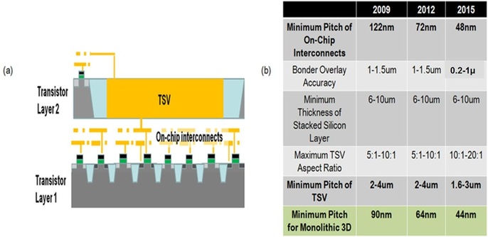
Comparison of Through-Silicon Via (TSV) 3D Technology and Monolithic 3D Technology
The semiconductor industry is actively pursuing 3D Integrated Circuits (3D-ICs) with Through-Silicon Via (TSV) technology (Fig. 8(a)). As shown in Fig 8(b), the International Technology Roadmap for Semiconductors (ITRS) [1] projects TSV pitch remaining in the range of several microns, while on-chip interconnect pitch is in the range of 100nm. The TSV pitch will not reduce appreciably in the future due stacked silicon layer thickness [1]. While the micron-ranged TSV pitches are enough for stacking memory atop processors and memory-on-memory stacking, they may not be enough to significantly mitigate the well-known on-chip interconnect problems [1]. Monolithic 3D-ICs offer through-silicon connections with <50nm diameter and therefore provide 10,000 times the areal density of TSV technology.

