Monolithic 3D Inc., the Next Generation 3D-IC Company
  • Home
  • Technology
    • Technology
    • Papers, Presentations and Patents
    • Overview >
      • Background
      • Why Monolithic 3D?
      • Paths to Monolithic 3D
      • Applications
    • Ion-Cut: The Building Block
    • Monolithic 3D Logic >
      • RCAT
      • HKMG
      • Laser Annealing
      • RCJLT
      • 3D Embedded RAM
      • 3D Gate Array
      • FPGA
      • Ultra Large Integration - Redundancy and Repair
    • Monolithic 3D Memory >
      • 3D DRAM
      • 3D Resistive Memories
      • 3D Flash
    • Monolithic 3D Electro-Optics >
      • 3D Image Sensors
      • 3D Micro-Displays
  • 3D-IC Edge
    • 3D-IC Edge
  • News & Events
    • News & Events
    • S3S15 Game Change 2.0 Video/P
    • Webcast
    • Webinar
    • Press Releases
    • In the News
    • Upcoming Events
  • About Us
    • About Us
    • History
    • Team
    • Careers
    • Contact Us
  • Blog
  • Simulators


Logic Gate Model


Picture
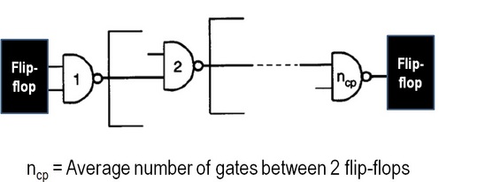
Fig. M4: Logic path model.

Logic gate paths are modeled as multiple stages of 2-input NAND gates between flip-flops, as shown in Fig. M4. An average length wire, whose length is determined from the wire length distribution model, exists between two NAND gate stages. NAND gate sizes are determined based on these conditions, using the equations shown in Fig. M5. While this is an approximate method to obtain logic gate sizes, area and power, it is simple and widely-used and is therefore adopted for IntSim v2.0. Please see [15][18] for more details of this model. 

Picture
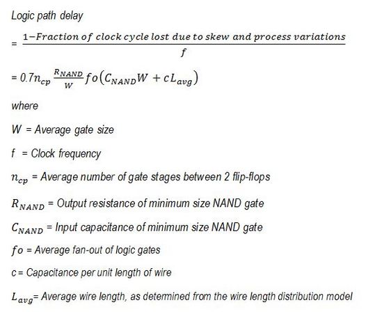
Fig. M5: Equations for determining average gate size.


© Copyright MonolithIC 3D Inc. , the Next-Generation 3D-IC Company, 2012 - All Rights Reserved, Patents Pending