Intermediate and Semi-Global Interconnect Model
A 2D-IC, or each device layer of a 3D-IC, in IntSim v2.0 has its own set of intermediate and semi-global interconnects. The wire pitches of these interconnect levels are obtained using the equations shown in Fig. M12. Essentially, The right hand side of Eq. (1) denotes the area required for routing wires in a pair of wire levels, and the left hand side denotes the area available for routing. Here, P is the pitch of the pair of wiring levels. Eq. (2) and Eq. (3) represent the condition that the delay of the longest wire in a pair of metal levels should be a certain fraction of the clock period, as discussed in [24]. For short-wires whose delay is typically logic gate dominated, this fraction is set as 0.25, and for long-wires whose delay is wire dominated, this fraction is typically around 0.8-0.9. Eq. (2) represents this criterion when no repeaters are inserted while Eq. (3) represents the case when repeaters are inserted with the Energy-Delay Product minimization strategy discussed in the repeater models section. Width of wires is equal to spacing between wires.
The wiring efficiency factor for intermediate and semi-global levels has two sources. The first source is via blockage due to vias to higher levels of metal and due to repeaters. These are modeled based on [27]. The second source is power via blockage that is modeled based on [26]. Wire resistivity increases due to size effects are modeled as shown in [26].
The wiring efficiency factor for intermediate and semi-global levels has two sources. The first source is via blockage due to vias to higher levels of metal and due to repeaters. These are modeled based on [27]. The second source is power via blockage that is modeled based on [26]. Wire resistivity increases due to size effects are modeled as shown in [26].
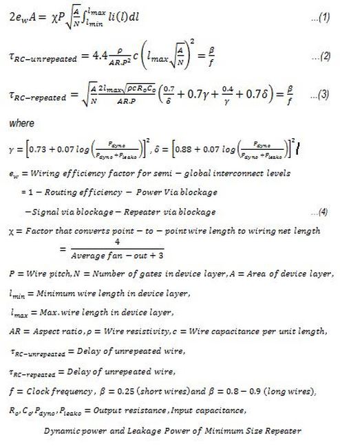
Fig. M12: Intermediate and semi-global interconnect model.