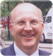
Albert K. Henning
Chief Scientist

Albert K. Henning has over thirty years’ experience in semiconductor device physics, and in micro- and nano-systems technology development. He specializes in technology and intellectual property development and assessment, related to semiconductor device physics, MEMS, microfluidics, and nanoscale technologies (nanotechnology).
Dr. Henning began his carrier as a Research Assistant for the Department of Physics and Astronomy at Dartmouth College from 1977 to 1979. Subsequently he served three years as a Device Physicist at Intel Corporation in Santa Clara, California, leading the device physics effort on Intel’s first CMOS process technology, used to build the 80386 microprocessor. He then returned to graduate school at Stanford University for five years, researching hot carrier device physics (and related temperature effects) in Si and SiGe MOSFETs under the direction of Jim Plummer. Over the next nine years he was Assistant and Associate Professor at the Thayer School of Engineering at Dartmouth College. His research centered on MOSFET device physics, TCAD, and metrology (including scanning Kelvin probe, scanning capacitance, and atomic force microscopies used to measure nanoscale dopant distributions in semiconductors), and microfluidic MEMS devices and process technologies.
In 1996 Dr. Henning started work at Redwood Microsystems as Director of Technology. Here he directed all aspects of research, development, and deployment of MEMS-based flow control systems, using silicon microvalves and related flow and pressure sensors, for customers such as Applied Materials, until December 2005.
He then founded Aquarian Microsystems in 2006, continuing to develop microfluidic and microflow devices and products. He was a finalist in the Clean Tech Open in both 2006 and 2007.
In 2007 he joined NanoInk, Inc. as Director of MEMS Technology. He conducted research on Dip Pen Nanolithography and NanoEncryption technologies, with applications to: verification of pharmaceutical (drug) authenticity; integrated circuit mask repair; and biosensor nano-array assay for disease diagnostics and drug development. He also directed development of microdevices and microsystems, based on atomic force microscopy and nanofluidics, and all metrology activities relative to micro- and nano-fabrication processes.
Dr. Henning has been granted 14 U.S. patents and patent applications. He has authored over 70 refereed journal, and conference proceedings, articles.
Dr. Henning received the AB in Physics (magna cum laude, 1977) and the AM in Physics (1979) from Dartmouth College, and the Ph.D. (Electrical Engineering, 1987) from Stanford University. He is a Senior Member of IEEE (2007).
