It is commonly believed that the fundamental limit to MOSFET feature-size scaling is direct source-drain tunneling. We may hit this limitation around the 5nm node. Is that the end of the road for CMOS Scaling?
Last week, during a dinner conversation with colleagues, the topic of scaling limits came up. Hmmm... I thought. Let me study this issue.
Prevailing Opinion
CMOS scaling limits have been a much researched issue. Figure 1 is a summary of analyses from various well-known folks in the semiconductor community. They all believe direct source-drain tunneling is the fundamental limiter to MOSFET feature-size scaling. These analyses were presented in top forums in our industry, such as the International Solid State Circuits Conference (ISSCC), the International Electron Devices Meeting (IEDM) and the Proceedings of the IEEE.
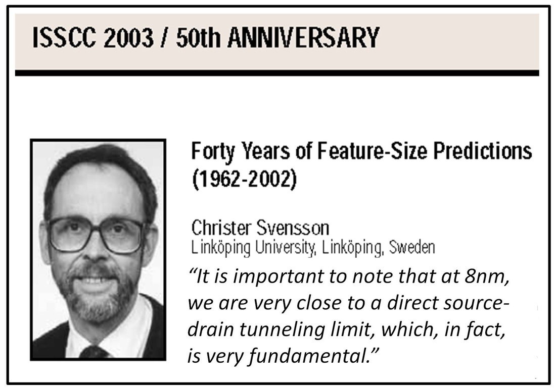
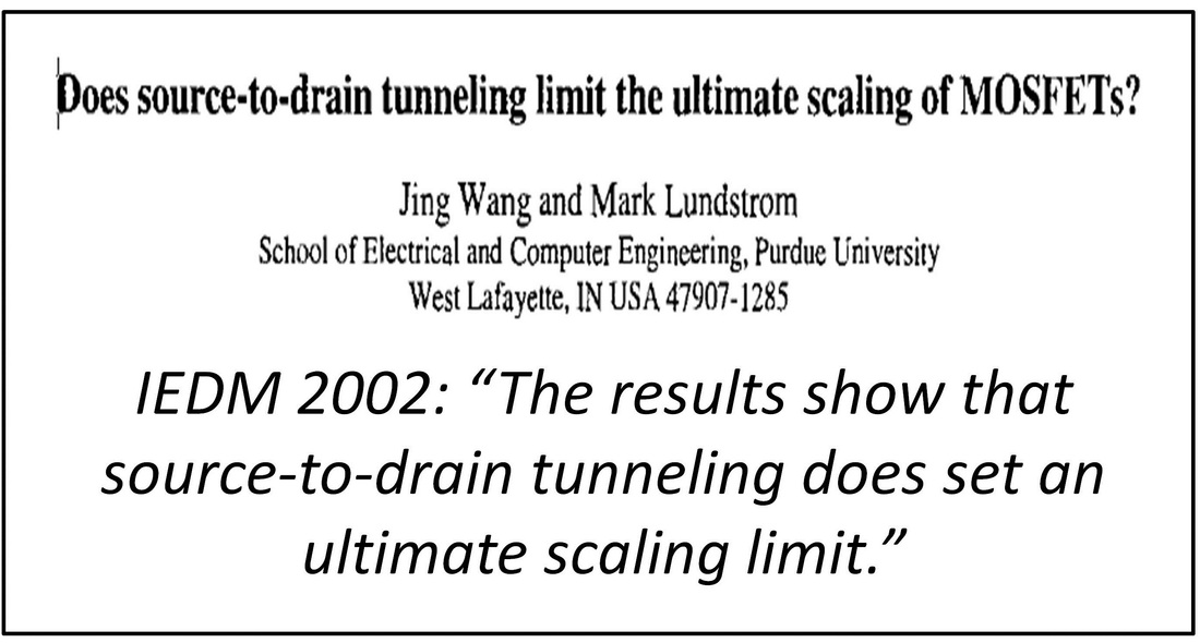

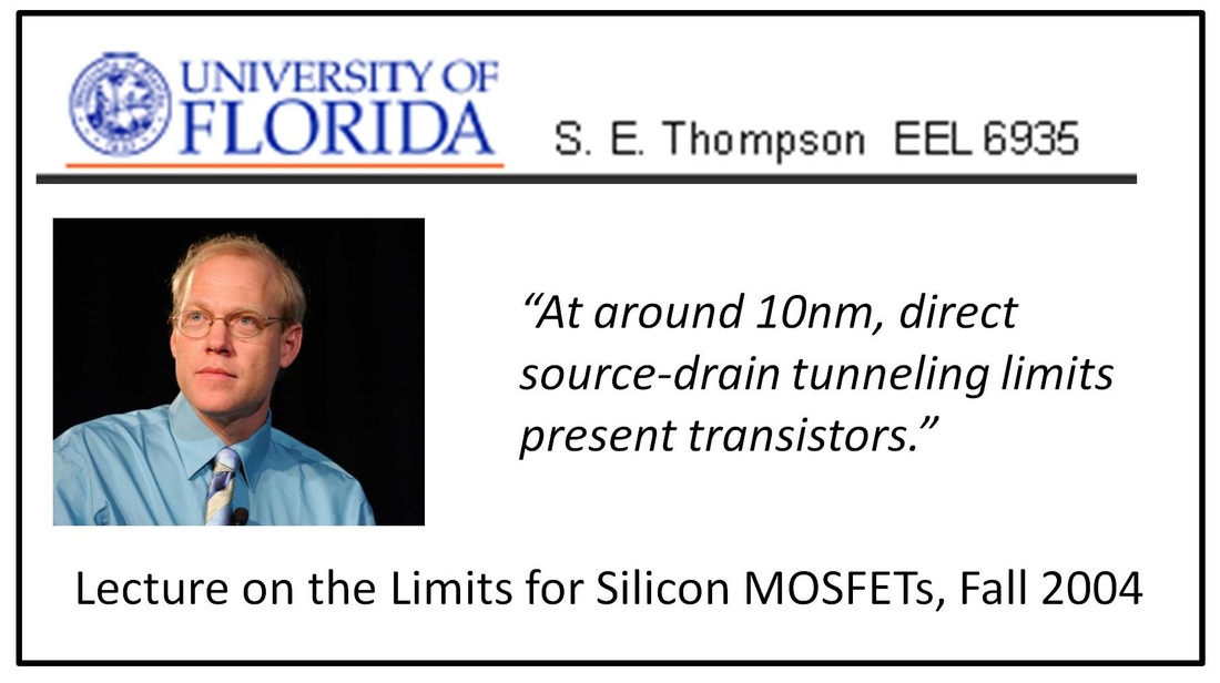
Figure 1: MOSFET scaling faces fundamental limitations with direct source-drain tunneling, say experts.
Understanding Direct Source-Drain Tunneling and the Limitation it Poses
When a transistor is OFF, there exists a potential barrier between the source and the drain, as shown in Figure 2. Leakage in present-day (22nm channel length) transistors is predominantly thermal assisted. For really small channel lengths (<10nm) though, one could have direct quantum-mechanical tunneling from the source to the drain. Figure 2 shows an equation for direct source-drain tunneling, which depends on:
When a transistor is OFF, there exists a potential barrier between the source and the drain, as shown in Figure 2. Leakage in present-day (22nm channel length) transistors is predominantly thermal assisted. For really small channel lengths (<10nm) though, one could have direct quantum-mechanical tunneling from the source to the drain. Figure 2 shows an equation for direct source-drain tunneling, which depends on:
- Width of the barrier, which is the channel length
- Height of the barrier, and
- Effective mass of carriers, which is a property of the transistor material
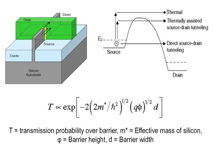
Figure 2: Direct source-drain tunneling phenomena
Figure 3 shows the effect of direct source-drain tunneling on a Finfet. Beyond 5nm channel length, almost all the off-state leakage is due to direct source-drain tunneling, and sub-threshold slope degrades to ~300mV/decade due to this effect. As most device physicists know, such high sub-threshold slope numbers are impractical. Since direct source-drain tunneling has such serious repercussions and there is not much scope to engineer around it, it is considered a fundamental issue and is believed to limit minimum feature size of silicon MOSFETs to around 5nm.
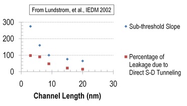
Figure 3: The limitations posed by Direct Source-Drain Tunneling
Is CMOS transistor miniaturization going to end around the 5nm node, or is there a way out?
Those of us working on semiconductors and chip design know most problems in our field can be solved, however daunting they might appear at the beginning. I spent some time thinking about the direct source-drain tunneling problem last week, and believe there is a solution. We may be able to scale CMOS logic transistors beyond the 5nm node, and it doesn't require any rocket science. Let me show you how...
Around the 90nm node, the DRAM industry had to figure out ways to reduce transistor feature sizes without running into leakage limitations. They started using an interesting device structure called a recessed channel MOSFET (Figure 4). In this device, the effective channel length is longer than the minimum feature size. For example, at the 90nm node, the transistor's effective channel length could be 180nm. So, one gets the density benefits of scaled feature sizes, and at the same time, leakage issues, which are crucial to DRAM, are avoided. Samsung, Hynix and Micron have manufactured this device for DRAM chips for around 5 years now. At the 2003 Symposium on VLSI Technology, Samsung reported that these devices offered 10x lower leakage, similar drive currents and higher gate capacitance compared to planar transistors. The chances are that you own a billion of these recessed channel devices, and are using them for the DRAM of your computer!
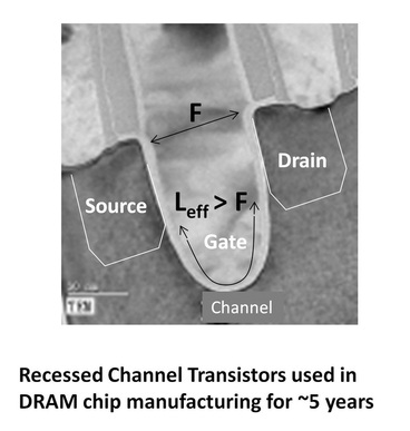
Figure 4: A TEM of a Recessed Channel Transistor.
You've probably figured out where I'm heading. For CMOS logic transistors, when we approach the direct source-drain tunneling limit, we could move to recessed channel devices and use channel lengths longer than the minimum feature size. This could allow us to continue miniaturization and increase component density. For example, at the 5nm node, we could have a 8nm channel length transistor without sacrificing density. Recessed channel devices also enable us to address issues with short channel effects such as Drain Induced Barrier Lowering (DIBL). Furthermore, moving to recessed channel devices could enable easy implementation of Monolithic 3D-ICs. See this page for more details. Next-generation logic transistors such as Finfets can be constructed with recessed channel topologies too. Hynix has done a lot of work on recessed channel Finfets for DRAM. Other high-density device structures where channel length is longer than the minimum feature size exist, such as vertical transistors. These are being actively explored by the DRAM industry too.
Conclusion: It certainly looks like we might be able to miniaturize CMOS technologies beyond the 5nm node someday.
Caveats
My conclusion above comes with a few caveats:
Conclusion: It certainly looks like we might be able to miniaturize CMOS technologies beyond the 5nm node someday.
Caveats
My conclusion above comes with a few caveats:
- NAND flash memory manufacturers such as Toshiba, Samsung and Micron scale the fastest in our industry. Due to the litho challenges they've hit, these companies are looking at alternative ways to get the benefits of scaling without lowering feature sizes. They've identified monolithic 3D as one way to do this (Figure 5). In fact, I hear one of these manufacturers is buying tools from equipment vendors to go to risk production with monolithic 3D in 2-3 years time! It remains to be seen whether similar approaches will be adopted for logic. If so, the logic industry may not need to move beyond the 5nm node in the next two decades.
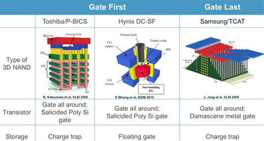
Figure 5: The NAND flash industry has monolithic 3D on their roadmap in the next 2-3 years.
- Notice how I said we may cross the 5nm node someday in my statement above. I did not say we would cross it with a 2 or 3 year cadence. This is mainly due to issues with lithography. ASML has more than 75% market share in immersion lithography and has a dominant position in EUV too. Having (almost) a sole supplier situation for what is probably the most important part of our industry is unfortunate. A sole supplier, due to lack of competition, can charge huge prices for his tools and is not penalized (much) for delayed product launches. Israel Beinglass' recent blog-post talked about ASML's revenue growing much faster than the rest of the equipment industry due to their high tool prices. Lack of competitive, timely and affordable litho technology can cause Moore's Law to slow down or can cause manufacturers to complement feature size scaling with approaches such as monolithic 3D.
- Devices such as recessed channel transistors or vertical transistors form just one possible solution to the direct source-drain tunneling issue. Other (possibly better) solutions could exist. The key point is that the direct source-drain tunneling limit may not be as fundamental as we think.


 RSS Feed