The Path Forward – 3D Integration with Hybrid Bonding
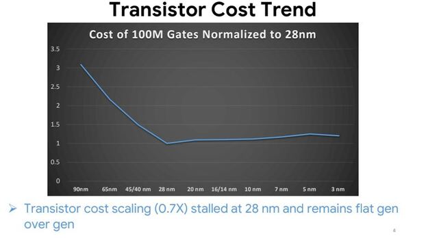
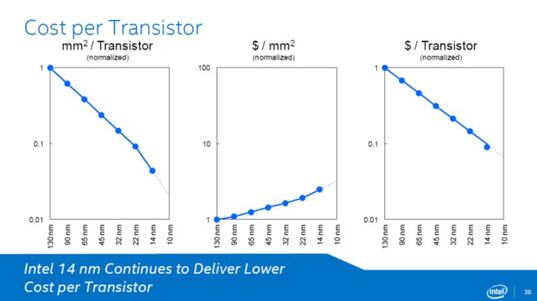
In the dynamic field of semiconductor technology, the ongoing discourse surrounding Moore's Law has experienced a notable evolution, prominently featuring Zvi Or-Bach's (MonolithIC 3D’ CEO) 2014 assertion. His statement that transistor cost scaling reached a pivotal juncture at 28 nm has attracted significant attention. The statement was recently validated by Milind Shah from Google in the Short Course (SC1.6 ) at IEDM 2023. The unequivocal statement, "Transistor cost scaling (0.7X) stalled at 28 nm and remains flat gen over gen”, confirms what was initially foreseen in earlier public viewpoints and blogs in 2014 predicting the conclusion of Moore's Law.
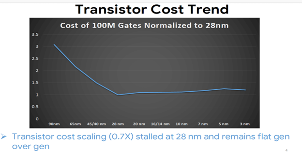
Source: Google, IEDM23 S.C1.6
Despite the stalling of cost scaling, why is the industry still pushing for ever-smaller transistors, aiming for a mind-boggling 1 nm node? The answer lies in system-level benefits. As illustrated by this chart from Bill Dally, Chief Scientist at NVIDIA
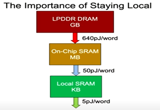
Source: Bill Dally, Berkeley EECS, Nov 30, 2022.
This, in turn, drives the trend of leading computing devices like CPUs and GPUs reaching reticle size and beyond. The pursuit of ever-smaller nodes allows for even tighter integration of components on the chip, further boosting performance and efficiency.
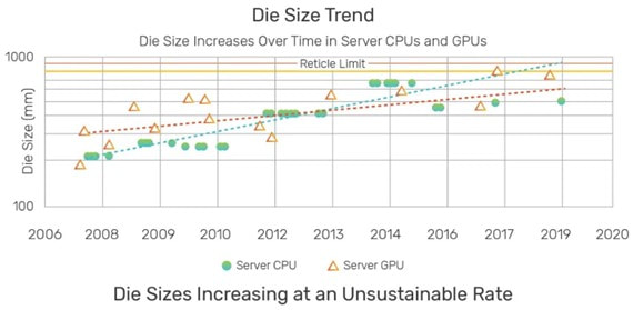
Source: AMD
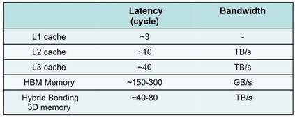
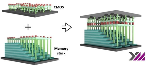
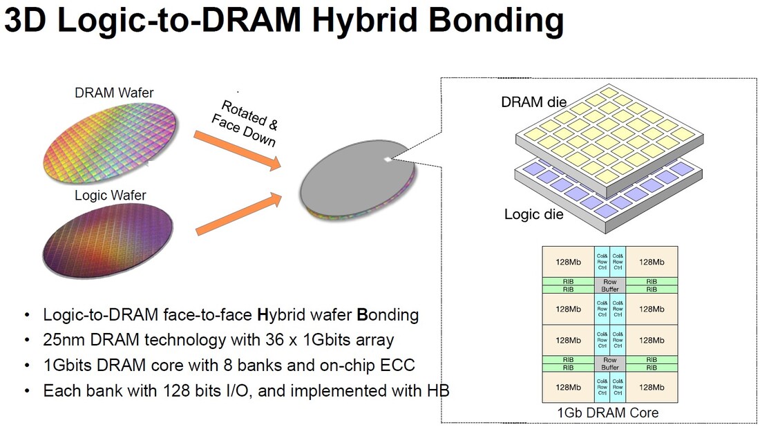
Unfortunately, logic and memory (DRAM, NAND) fabrication processes is very different. Accordingly, they are produced on different wafers and cannot be integrated by scaling. And making it even worse SRAM bit-cell scaling had stopped at the 5 nm node.
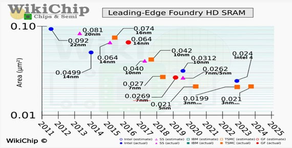
Source: WikiChip
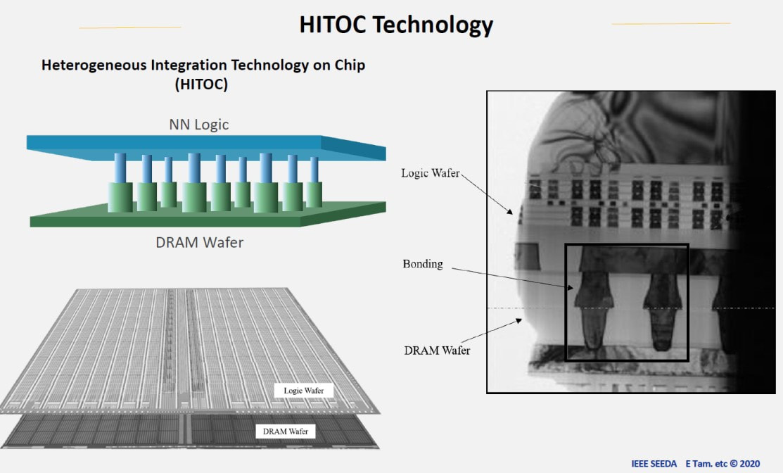
It seems that both AMD and TSMC understood these trends and during the last couple of years adapted Hybrid Bonding technology to enable future progress in computing performance.
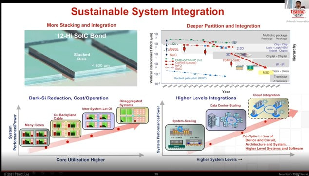
Source: TSMC
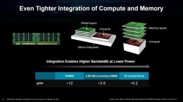
Source: Dr. Lisa Su AMD ISSCC 2023 Tighter Integration Of Compute And Memor
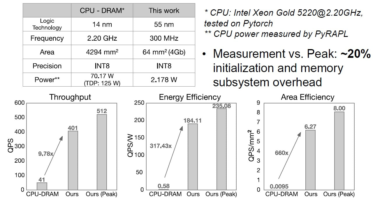
While current implementations like AMD's 3D V-Cache represent a stepping stone towards the full potential of 3D integration, significant hurdles remain. These include a fundamental shift in architectural thinking, moving from traditional edge interconnect to a novel 3D integration approach. Furthermore, achieving widespread adoption will require innovations in system-level redundancy, wafer-scale integration, and even on-chip RF networks. For a glimpse into this ambitious vision, look no further than Chapter 15* of the NANO-CHIPS 2030 book, aptly titled "A 1000× Improvement of the Processor-Memory Gap."(*Download the chapter here)


 RSS Feed