2nd edition of: "Dimensional Scaling and the SRAM Bit-Cell"

We have a guest contribution from Zvi Or-Bach, the President and CEO of MonolithIC 3D Inc. Zvi adds information to his previous blog post: Dimension Scaling and the SRAM Bit-Cell.
I just downloaded the ASML presentation from Semicon West2013 site - ASML's NXE Platform Performance and Volume Introduction. Slide #5 - IC manufacture's road maps - says it all.
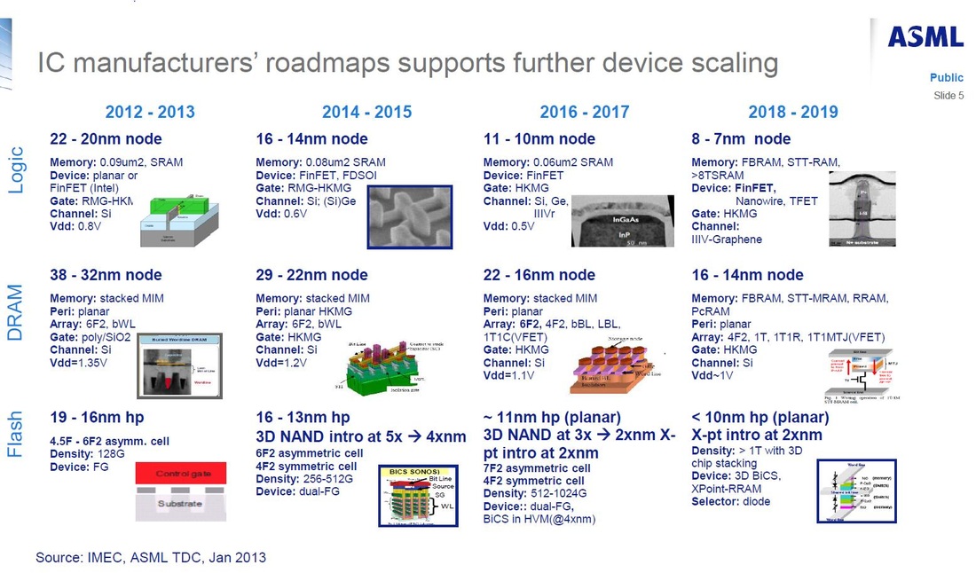
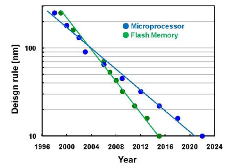
Embedded SRAM will scale from 0.09µm² at 22-20nm node to 0.06µm² at 11-10nm node. In other words only 30% reduction instead of the 4x reduction expected of historical dimension scaling, to roughly 0.02µm²!!!
In our previous blog (attached below) that followed ISSCC 2013 we saw some early indication of this slowdown. Yet we were still surprised to realize how bad it really is. This might explain why after resisting IBM and other pushes for embedded DRAM, Intel announced few month ago that its Haswell processor will incorporate embedded DRAM after all.
Another point from this ASML slide is the adaption of monolithic 3D by the NAND Flash vendors. We believe this is a start of a trend, and that logic vendors has now one more reason to follow it.
Previous Blog:
One Thing that ISSCC 2013 Highlighted to Us
Dimensional Scaling and the SRAM Bit-Cell
The IEEE International Solid-State Circuit Conference Feb 17-21, 2013 just ended in San Francisco last week, and the issue of dimensional scaling as it relates to EUV and future per transistor device cost was an important topic in the plenary session. One important, and perhaps overlooked, aspect of the industry’s scaling issue relates to the future of the SRAM bit-cell within this framework of dimensional scaling. We would like to shine some light on this impending issue.
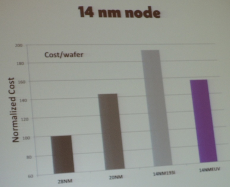
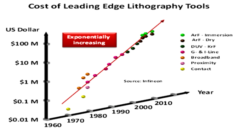
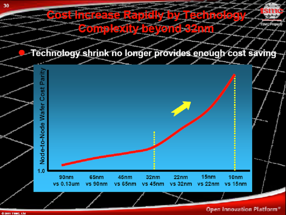
As widely reported in the industry and articulated by ASML’s Executive VP & CTO Martin van den Brink at ISSCC 2013, there is substantial evidence that without EUV the cost of logic transistors is most likely going up with scaling. One slide he used to illustrate this is below:
As widely reported in the industry and articulated by ASML’s Executive VP & CTO Martin van den Brink at ISSCC 2013, there is substantial evidence that without EUV the cost of logic transistors is most likely going up with scaling. One slide he used to illustrate this is below:

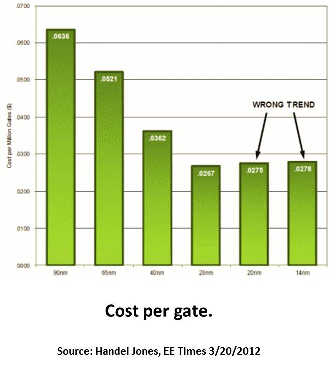
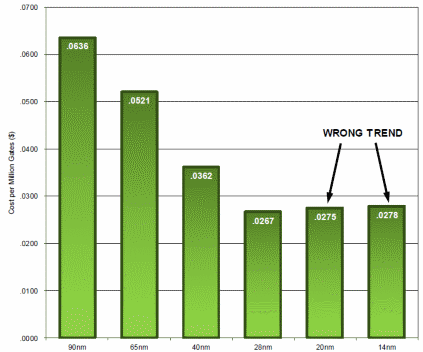
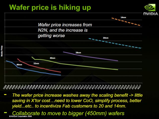
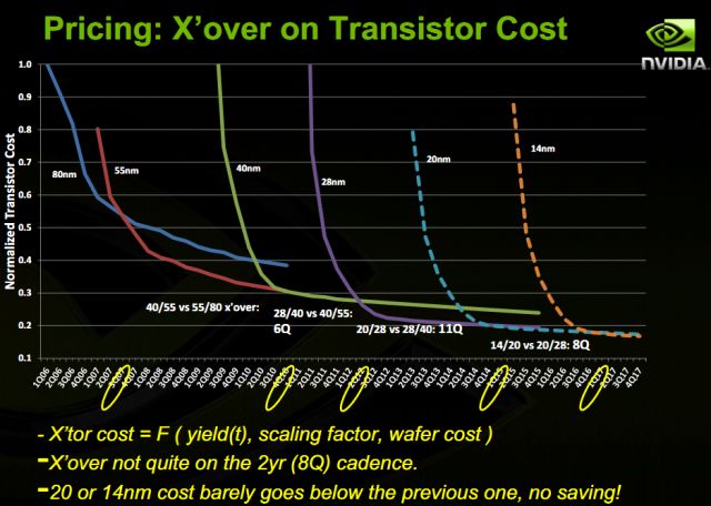
The above slide arrived after Martin had presented another non-encouraging slide, showing the same view from three companies: a Broadcom chart of increasing cost per gate correlated with dimensional scaling, together with the now famous Nvidia chart of no more crossover of transistor cost below 28nm, and third a GlobalFoundries chart showing some limited value for EUV.
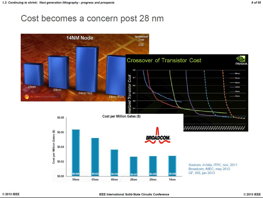
We may attribute Martin statements to ASML interest in promoting EUV, but since ASML has already received significant EUV participation from INTEL, Samsung and TSMC, it might indicate further bumps are on the road to bringing EUV to market. We don't know if EUV will ever become real, but we do know very well that it is been delayed, and delayed again, and delayed again. It was made public recently that EUV has probably already missed the 10nm process node -“10nm will be optical,†said Ajit Manocha, chief executive of GlobalFoundries.
An even more interesting slide was presented by van den Brink:
An even more interesting slide was presented by van den Brink:
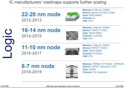
This chart brings up an important aspect of dimensional scaling that has not been discussed much before - the scaling of the SRAM bit-cell. According to this chart, the SRAM bit-cell size might not be reduced from the 20nm to 10 nm node, and might even get larger at 7nm as it may need more than 8 transistors. (Sound familiar? Fabs are doing the same with BEOL metallization scaling…little or none)
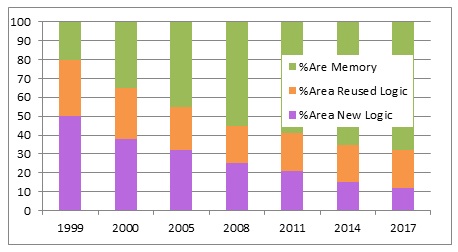
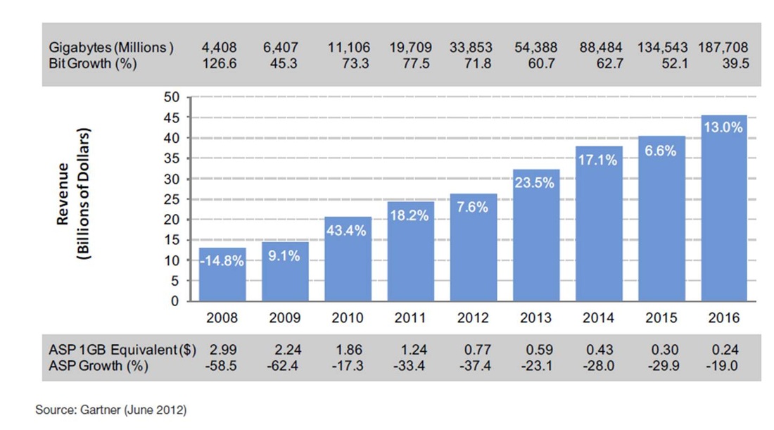
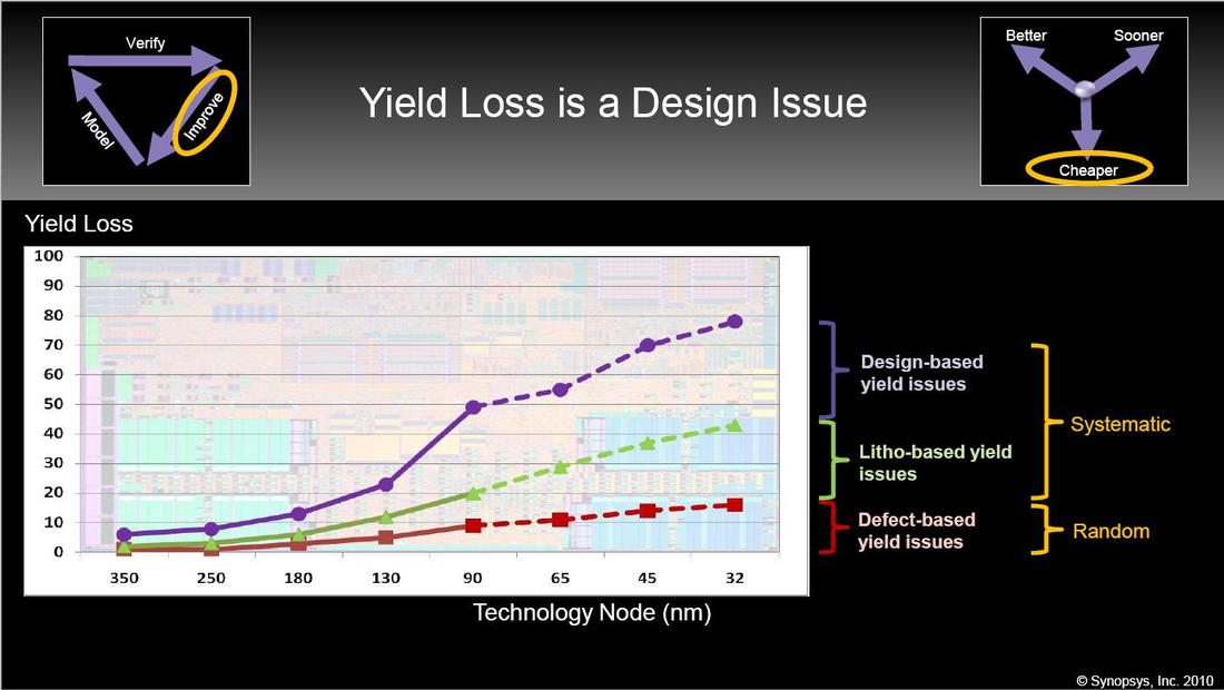
Modern logic devices demand a significant amount of embedded SRAM. In fact, more than 50% of the typical logic device area is allocated for these SRAM as illustrated by the following chart of Semico (June, 2010)
Modern logic devices demand a significant amount of embedded SRAM. In fact, more than 50% of the typical logic device area is allocated for these SRAM as illustrated by the following chart of Semico (June, 2010)
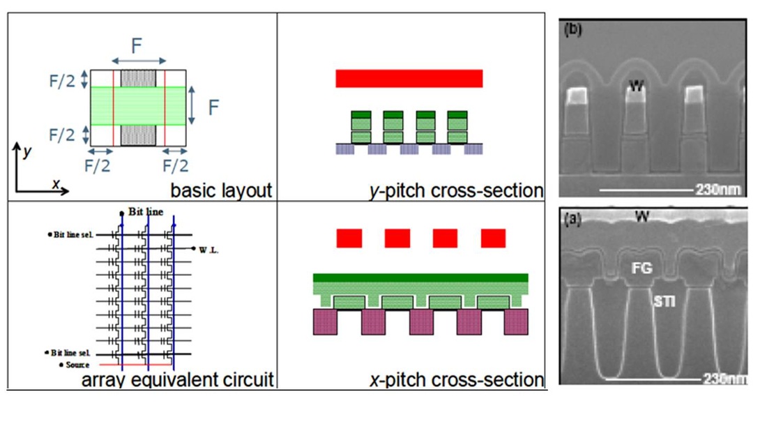
The dominant embedded SRAM bit-cell architecture has been the 6 transistor cell (6T). And for many years this very cell has been hand-crafted using special design rules independently developed by foundries for every new technology node. It makes sense: the SRAM cell is a unique structure that does not obey normal logic design rules as it drives output against output anytime a write cycle is being performed. In many cases it is the SRAM cell that is the most sensitive portion of the logic device to process parameter variations and this sensitivity greatly impacts end device yield.
It well known that scaling the SRAM bit-cell has become harder and harder. Some vendors have already moved away from the 6T bit-cell in preference to the 8T (eight transistors) bit-cell. ISSCC 2013 had a significant number of papers that were presented using 8T SRAM. The few papers who kept the 6T SRAM embedded in their logic devices were forced to add read/write support circuits and additional overhead to enable the 6T bit-cell to function reliably.
Since SRAM bit scaling is now not able to keep up with logic scaling, the overall end device cost scaling could be even more disappointing than the transistor or gate cost illustrations above.
Of course, well aware of this trend, IBM has been promoting their embedded DRAM solution for years. In the recent Common Platform Forum Dr. Gary Patton, VP, IBM Semiconductor R& D Center, was very pleased to share that in their 32nm product line the use of the embedded DRAM has given IBM the equivalent of a process node scaling benefit. Yet, as of now, most other vendors have not adopted eDRAM due to the process complexity and cost it adds to the logic process. It fair to assume that the appetite for eDRAM will not grow with dimensional scaling as the DRAM capacitor will be very hard to scale, the extra power for supporting DRAM will not be available and the cost of advance process development to add in extra complexity will be too high.
Accordingly we can learn from the recent ISSCC that dimensional scaling is facing the cost challenges we were aware of before in addition to new challenges that we might not have been aware of: the cost and the active/passive power handicaps due to the incompatibility of the 6T SRAM bit-cell with scaling.
As we have suggested before, now that monolithic 3D is practical, we could advance and maintain Moore's Law by augmenting dimensional scaling with 3D IC scaling. We could enjoy depreciated equipment charges for more years and much lower R&D engineering outlays that would bring down production and development costs, and also enjoy improvements to power and performance.
Another exciting option is to replace the 6T SRAM bit-cell with the 1T bi-stable floating body memory cell invented by Zeno Semiconductor. The Zeno bit-cell provides two stable states, analogous to an SRAM while only consuming ~20% area of a traditional 6T SRAM and requires considerably less power. The area and power savings over a traditional 6T SRAM improve further with scaling. Most excitingly the Zeno bit-cell is compatible with existing logic processes.


 RSS Feed