
We have a guest contribution today from Brian Cronquist, MonolithIC 3D Inc.'s VP of Technology & IP. Brian discusses low temperature cleaving.
Thanks to everybody who came by our booth at SemiconWest SemiconWest 2012 this second year! We really enjoyed talking with you about all the exciting possibilities for new products and processes that are enabled by monolithic 3D IC.
For those who could not make it, here is what our booth looked like:
For those who could not make it, here is what our booth looked like:
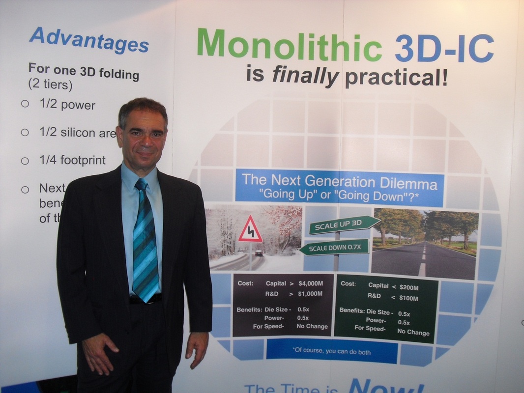
Nice tie again Zvi! You can still visit us at www.monolithic3d.com.
The most common area that you asked us was about low temperature (less than 400°C) bonding and low temperature cleaving processes. The two topics are quite inter-related: One must make the bond stronger than the energy it takes to cleave at the plane you want, rather than cleave at th at fresh bond. In October last year I wrote a blog about the many low temperature bonding techniques and strategies available and their respective bond strengths. Today, I would like to briefly address some of the low temperature cleaving methods available. Generally they involve either a mechanically induced (blade, gas jet, water jet) method, a lower temp thermal (co-implantation, microwave, etc.) cleaving/layer-transfer method, or a combination of both.
Here are a few papers, with some industrial announcements at the end.
One of the earliest methods published is co-implantation by Q.Y. Tong et al. of Duke University at the 1997 IEEE SOI Conference. Tong could greatly affect the kinetics of the hydrogen blister formation by co-implantation of Boron. They were able to transfer a 0.4um silicon layer onto a quartz substrate with a 150°C exposure to the quartz by pre-annealing the co-implanted silicon for 10 minutes at 250°C.
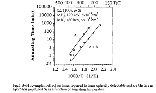
Figure 1
Tong with colleagues at the Max-Planck-Institute followed up with more co-implantation
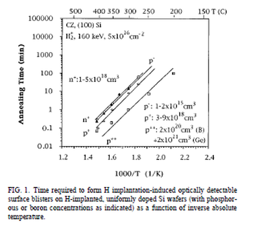
Figure 2
kinetics data in a 2008 Applied Physics Letter. They again demonstrated a 200°C silicon cleave.
In 1998 App. Phys. Lett., Agarwal et al. showed that He implanted with the H could lead to a significant decrease in the total implant fluence (and hence cost) necessary to achieve Si layer transfer. The total implantation dose can be three times smaller than that which is necessary using H alone.
In 1998 App. Phys. Lett., Agarwal et al. showed that He implanted with the H could lead to a significant decrease in the total implant fluence (and hence cost) necessary to achieve Si layer transfer. The total implantation dose can be three times smaller than that which is necessary using H alone.
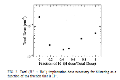
Figure 3
Nguyen et al. of Soitech/CEA-Leti, at the 2003 IEEE SOI Conference showed that He co-implantation could be used to control the kinetics, so time, dose and temperature trades could be made.
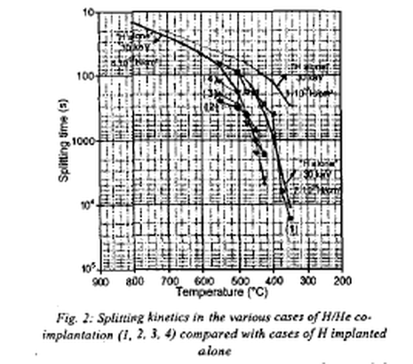
Figure 4
Ma, et al. showed in Semcond Sci. Technol. 2006 that a co-implanted cleave has a smoother
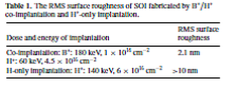
Figure 5
surface than a hydrogen-only implanted cleave.
In 2000 App. Phys. Lett., Henttinen et.al showed mechanical cleaving, blade or N2 gas, on low temperature bonded silicon wafers (ox-ox bond). Depending on the H dose, Henttinen could
In 2000 App. Phys. Lett., Henttinen et.al showed mechanical cleaving, blade or N2 gas, on low temperature bonded silicon wafers (ox-ox bond). Depending on the H dose, Henttinen could
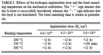
Figure 6
cleave the silicon wafers at 200°C or 300°C. Henttinen et.al followed up later in 2002 in J. Nucl. Instr. and Meth. in Phys with fundamental mechanistic studies and also demonstrated that with enough B doping one can enable H-implanted layer exfoliation below 200°C.
Cho et al., in 2003 App. Phys. Lett. reported that full wafer layer transfer could be achieved with a mechanical cleave (edge initiated crack propagation) after a 250°C annealing that enabled the bonding strength at the acceptor/donor interface to exceed the required cleave energy at the hydrogen implant plane.
En, et al., of Silicon Genesis, described a room temperature H implant using PLAD (Plasma Immersion Ion Implantation), plasma assisted oxide to oxide bonding, and a room temperature mechanical cleave process at the 1998 IEEE SOI Conference.
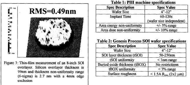
Figure 7
Current, et al. of Silicon Genesis, showed a wafer separation tool in MRS 2001 where they utilized a pressurized N2 jet to cleave silicon bonded pairs at room temperature.
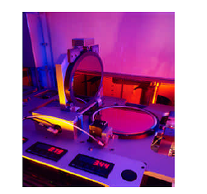
Figure 8
Recently from the industrial side:
Soitec announced at SemiconWest 2012 the availability of a room temperature smart cut:
"Soitec’s low-temperature Smart Cut process uses oxide-oxide molecular bonding and atomic-level cleaving to transfer mono-crystalline silicon films as thin as 0.1 micron onto partially or fully processed wafers. On this new material layer, a second level of devices can be processed and this integration can be repeated in an iterative mode. Transferring an extremely thin layer enables higher interconnect density, higher signal throughput and simpler TSV processing. Benefits include increased computing bandwidth, lower overall manufacturing cost, and power savings due to the reduced wiring distance between connected devices. This final benefit is well suited for producing advanced memory or CMOS logic 3D IC systems.†See: http://www.soitec.com/en/news/press-releases/article-346/
SiGen (Silicon Genesis) has tools (some shown above) available that will bond and cleave at or near room temperature: http://www.sigen.net/semi_debondCleave.html
References:
TONG, Q.-Y., et al., "Low Temperature Si Layer Splitting", Proceedings 1997 IEEE International SOI Conference, Oct. 1997, pp. 126-127
TONG, Q.-Y., et al., "A ‘‘smarter-cut’’ approach to low temperature silicon layer transfer", Applied Physics Letters, Vol. 72, No. 1, 5 January 1998, pp. 49-51
AGARWAL, A., et al., "Efficient production of silicon-on-insulator films by co-implantation of He+ with H+'" Applied Physics Letters, vol. 72, no. 9, March 1998, pp. 1086-1088.
NGUYEN, P., et al., "Systematic study of the splitting kinetic of H/He co-implanted substrate", SOI Conference, 2003, pp. 132-134
MA, X., et al., "A high-quality SOI structure fabricated by low-temperature technology with B+/H+ co-implantation and plasma bonding", Semiconductor Science and Technology, Vol., 21, 2006, pp. 959-963
HENTTINEN, K. et al., "Mechanically Induced Si Layer Transfer in Hydrogen-Implanted Si Wafers," Applied Physics Letters, April 24, 2000, p. 2370-2372, Vol. 76, No. 17.
HENTTINEN, K. et al., "Cold ion-cutting of hydrogen implanted Si," J. Nucl. Instr. and Meth. in Phys. Res. B, 2002, pp. 761-766, Vol. 190.
CHO, Y., et al., “Low Temperature Si Layer Transfer by Direct Bonding and Mechanical Ion Cut,†Applied Physics. Letters., vol. 83, no. 18, November 2003, pp. 3827-3829.
EN, W. G., et al., “The Genesis ProcessTM: A New SOI wafer fabrication methodâ€, Proceedings 1998 IEEE International SOI Conference, pp. 163-164 (Oct. 1998).
CURRENT, M. I., et al., “Atomic-layer Cleaving and Non-contact Thinning and Thickening for Fabrication of Laminated electronic and Photonic Materialsâ€, 2001 Materials Research Society Meeting, April 16-20 2001, Paper I8.3.


 RSS Feed