
We have a guest contribution today from Paul Lim, who is a Principal Device Engineer at our company. Paul tells us some interesting info about MonolithIC 3D Inc.'s first commercial.
|
|
|
We have a guest contribution today from Paul Lim, who is a Principal Device Engineer at our company. Paul tells us some interesting info about MonolithIC 3D Inc.'s first commercial.
0 Comments
Ion-cut, the process used for manufacturing SOI wafers for the past 15 years, is the most popular method to form c-Si layers for monolithic 3D-ICs. In this blog-post, I'll share cost estimates for ion-cut, and explain why even price-sensitive markets such as solar are adopting it. For monolithic 3D, it is often required to form single crystal silicon above copper wiring layers at temperatures lower than 400C. Fig. 1 shows the ion-cut process, which is the most popular method of achieving this objective. Hydrogen is first implanted into a "top layer wafer" to create a defect plane. This "top layer wafer" is then flipped and bonded onto a "bottom layer wafer" having transistors and copper wiring.After this, the structure is cleaved at the defect plane using a 400C anneal or a sideways mechanical force. Finally, a CMP is done to get a good surface. 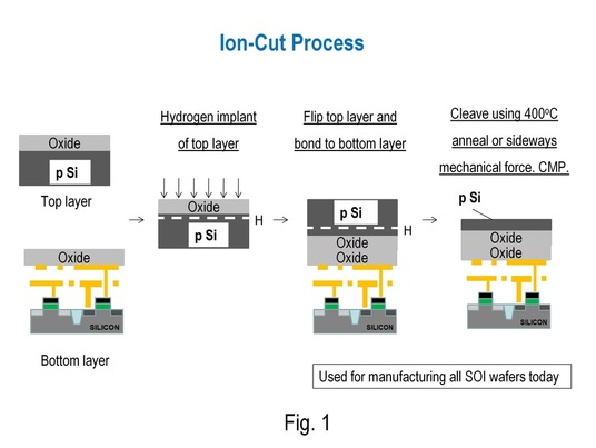
The previous paragraph explained how ion-cut can be used for stacking single crystal silicon layers for 3D-ICs. For forming a SOI wafer using ion-cut, the "bottom layer wafer" in Fig. 1 is a blank silicon wafer instead of a processed one with transistors and wires. As many of you know, ion-cut is the standard process used for high-volume manufacturing of SOI wafers today. Cost-of-Ownership Analysis Fig. 2 shows cost calculations for ion-cut using a Sematech Cost-of-Ownership framework. Tool prices and throughputs are obtained from equipment manufacturers who provide tools for these ion-cut process steps. The "top layer wafer" in Fig. 1 is re-used, as is typical in an ion-cut process. The total cost per wafer for a single ion-cut is $58, which is close to estimates that ion-cut practitioners in the industry have provided us. The number seems reasonable... this is what you'd expect of a process that doesn't involve any litho steps. In addition, with passage of time, one would expect throughput of various steps to improve significantly, bringing the price down further. 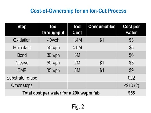
Companies such as Twin Creeks Technologies and SiGen are using ion-cut for the solar industry today (Fig. 3). As you'd know, the solar industry is a lot more cost-sensitive than the semiconductor industry... this application is possible mainly because these vendors are reaching costs similar to Fig. 2. 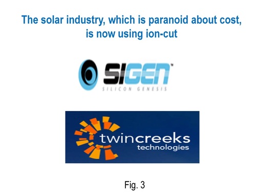
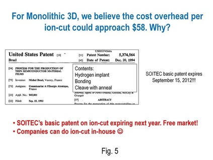
Hmmm... If the additional cost per wafer is $58, why are SOI wafers considered "costly" today? This is because of business issues with SOI wafer manufacturing (see Fig. 4). 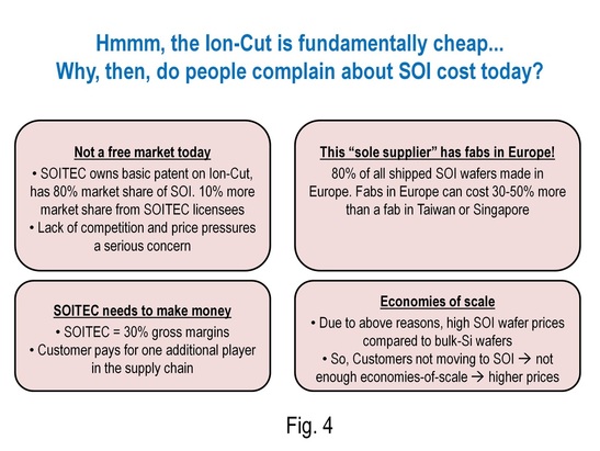
The price per ion-cut could be as low as $58, which is miniscule compared to wafer cost of a logic wafer (~$4000), NAND flash memory wafer (~$1500) or DRAM wafer (~$2000). This is encouraging for the monolithic 3D application, since ion-cut is the most popular technique to get stacked single crystal silicon layers. Once these stacked single crystal silicon layers are obtained, one can use MonolithIC 3D Inc.'s innovative device architectures to build high-quality 3D chips.  We have a guest contribution today from Israel Beinglass, the CTO of MonolithIC 3D Inc. Israel talks about the use of monolithic 3D integration for SRAM stacking above/below logic.  We have a guest contribution today from Brian Cronquist, MonolithIC 3D Inc.'s VP of Technology. He gives an update on our company's Semicon West activities. We had an exciting meeting last week with Fabian Pease, a Stanford University Professor who was one of the inventors of microchannel COOLing. Let me tell you about this meeting...
 We have a guest contribution today from Zvi Or-Bach, MonolithIC 3D Inc.'s President and CEO. Zvi talks about some good news we received from the Semicon West committee recently. All of us know Jerry Sanders' famous quote from the 1990s. "Real men have fabs", said the AMD CEO. Over the past decade, several famous companies, many of whom had real men, dumped their fabs and went fab-lite or fabless. I believe there will be a similar move towards the IP business model in the next decade. Here's why...
|
Search Blog
Meet the Bloggers    Follow us   Recommended LinksRecommended Blogs
Archives
January 2024
Categories
All
|
 RSS Feed