
We have a guest contribution today from Israel Beinglass, the CTO of MonolithIC 3D Inc. Israel discusses about TSVs.
Have you read some of the recent TSV headlines?
1. January 31, 2012 - CEA-Leti launched a major new platform, Open 3D, that provides industrial and academic partners with a global offer of mature 3D packaging technologies for their advanced semiconductor products and research projects.
2. March 7, 2012 - Semiconductor fab equipment supplier Applied Materials Inc. (AMAT) opened the new Centre of Excellence in Advanced Packaging at Singapore's Science Park II with its partner in the endeavor, the Institute of Microelectronics (IME)
3. March 26, 2012 - PRNewswire - Semiconductor design/manufacturing software supplier Synopsys Inc. (Nasdaq: SNPS) is combining several products into a 3D-IC initiative for semiconductor designers moving to stacked-die silicon systems in 3D packaging.
It is amazing that after so many years of development and efforts and great presentations we are still not in a full production and still basic R&D as well as EDA still in infancy.
Most people in the Industry consider Merlin Smith and Emanuel Stern of IBM the inventors of TSV based on their patent “Methods of Making Thru-Connections in Semiconductor Wafers†filed on December 28, 1964 and granted on September 26, 1967, as shown below patent number 3,343,256
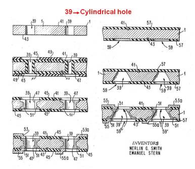
Figure 1: IBM TSV patent
In April 12, 2007 IBM announced a breakthrough new 3D technology:
Armonk, NY - 12 Apr, 2007: IBM (NYSE: IBM) today announced a breakthrough chip-stacking technology in a manufacturing environment that paves the way for three-dimensional chips that will extend Moore’s Law beyond its expected limits. The technology – called “through-silicon vias†- allows different chip components to be packaged much closer together for faster, smaller, and lower-power systems… IBM is already running chips using the through-silicon via technology in its manufacturing line and will begin making sample chips using this method available to customers in the second half of 2007, with production in 2008.
Armonk, NY - 12 Apr, 2007: IBM (NYSE: IBM) today announced a breakthrough chip-stacking technology in a manufacturing environment that paves the way for three-dimensional chips that will extend Moore’s Law beyond its expected limits. The technology – called “through-silicon vias†- allows different chip components to be packaged much closer together for faster, smaller, and lower-power systems… IBM is already running chips using the through-silicon via technology in its manufacturing line and will begin making sample chips using this method available to customers in the second half of 2007, with production in 2008.
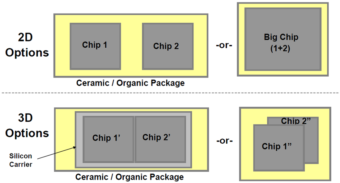
Figure 2: Original story on TSV advantages followed IBM announcement
Figure 2 is taken from Ignatowski’s presentation made shortly after IBM’s TSV announcement. This type of argument where chip stacking is compared to 2 chips side by side has become the corner stone of the TSV story (http://www.sematech.org/meetings/archives/3d/8334/pres/Ignatowski.pdf).
Already at that point (2007) it was clear to IBM that there were many issues with the technology that needed to be resolved. Figure 3 shows the IBM slide discussing some of the problems for implementing TSV for mass production.
Already at that point (2007) it was clear to IBM that there were many issues with the technology that needed to be resolved. Figure 3 shows the IBM slide discussing some of the problems for implementing TSV for mass production.
Figure 3: Issues per IBM with the TSV technology
During the years following and through to today there have been many attempts to bring the technology to the mass production. All have been without real success.
The professional literature is full of beautiful road maps showing how TSV is going to change the industry with “more than Moore†as the next scaling methodology.
Figure 4 is the Advanced Packaging road map for Texas Instruments which is typical of most companies Packaging/TSV road maps.
The professional literature is full of beautiful road maps showing how TSV is going to change the industry with “more than Moore†as the next scaling methodology.
Figure 4 is the Advanced Packaging road map for Texas Instruments which is typical of most companies Packaging/TSV road maps.
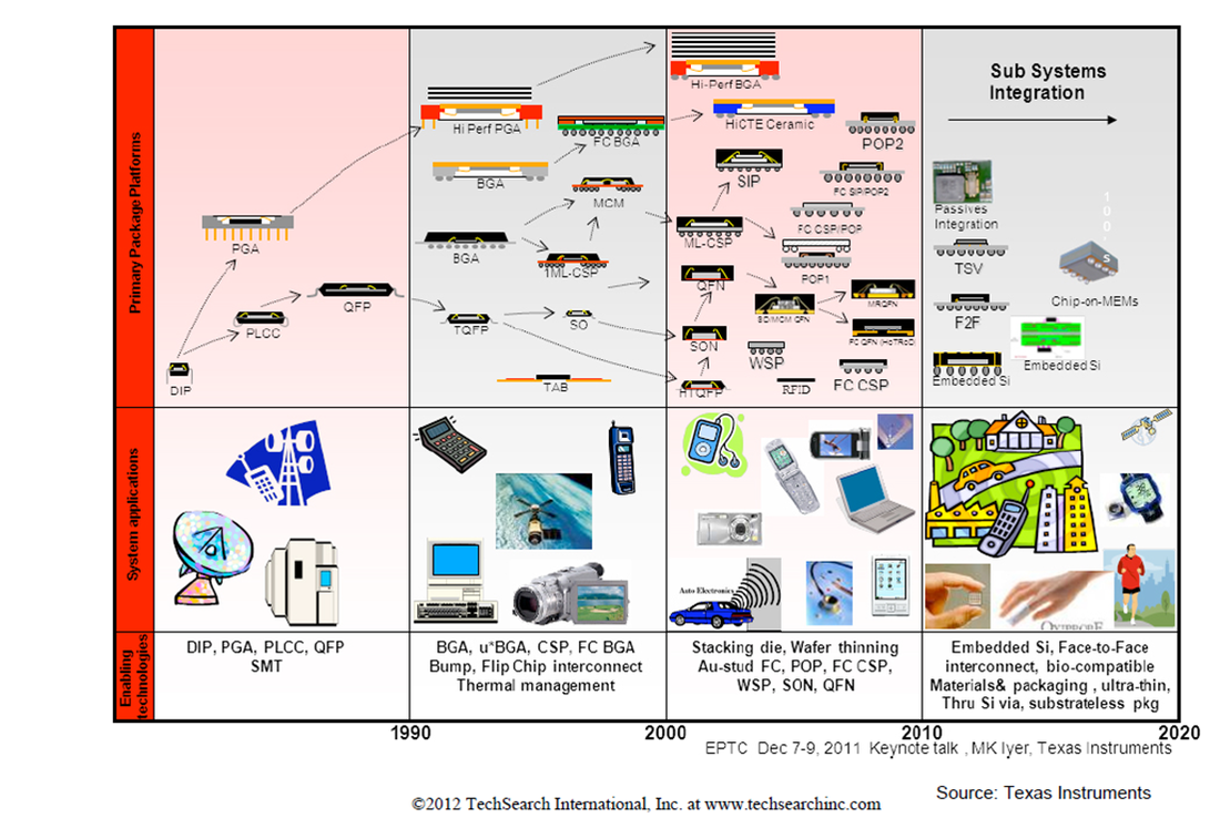
Figure 4: TI Packaging Technology Trends Dec 2011
There are several issues that are facing the industry when trying to implement TSV technology: (not in any specific order)
Process issues:
Design and EDA:
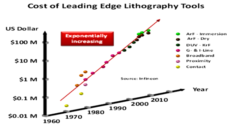
- Currently the cost associated with implementing TSV is at least for now higher than other solutions. This is hampering the motivation to develop and implement the TSV technology.
Also the CapEx to implement TSV needs to be addressed, Figure 5 is a table put together by ASE that shows the readiness of the various equipment needed to run a typical TSV process.
Process issues:
- Via etching and filling are extremely slow since the dimensions are very different from the “normal†dimensions the industry uses (single/multiple digit microns for depth and diameter vs. nanometers, plus aspect ratios>5)
- Via, first, middle or last which way to go? Each affects the whole process logistics in differing ways
- How to integrate wafers from different sources Logic from IDM and/or foundry and memory from a memory Fab
- Wafer thinning, how to handle fully processed wafer 20-80 micron thick including bonding and de-bonding. Rumors are that both Applied Materials and TEL are developing this kind of a tool
- Wafer-to-wafer (W2W) or die-to-wafer (D2W) bonding: each have processing challenges
- Singulation of the final product
- Substrate (carrier)for TSV
Design and EDA:
- Design rules are currently not compatible with TSV
- Who is responsible for the “system†design if there are several sources for product to be integrated?
- EDA is way, way behind
- Thermal simulation and heat removal issues
- Foundries/IDM vs. OSAT, who is doing what and who picks up yield loss
- Final test
- Reliability
- The major foundries have no memory knowledge or how to integrate the memory on top of logic
- Currently the cost associated with implementing TSV is at least for now higher than other solutions. This is hampering the motivation to develop and implement the TSV technology.
Also the CapEx to implement TSV needs to be addressed, Figure 5 is a table put together by ASE that shows the readiness of the various equipment needed to run a typical TSV process.
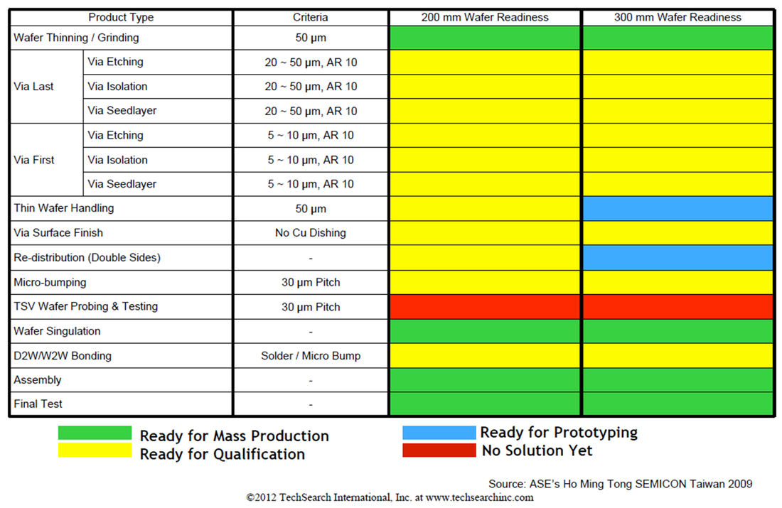
Figure 5: TSV equipment readiness per ASE
One of the key issues that some people are neglecting right now is the fact that we do have an interim solution to the problem. It may- probably not be the best solution and perhaps not the most elegant one but it does work. These are the variety of packaging techniques using chip on chip with wire bonding, and assortment solutions (PoP etc).
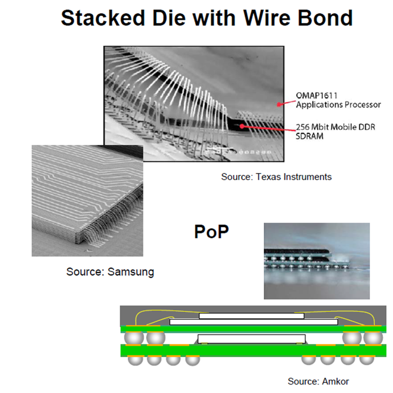
Figure 6: Alternative methods for 3D chip connectivity
The following are some of the comments made by industry experts over the last few months.
TSMC
Doug Yu’s keynote address at the 3D Architectures for Semiconductor Integration and Packaging Conference in December, he noted that TSMC intends to provide full 2.5F and 3D service including chip design and fabrication, stacking and packaging. Yu, who is senior director of integrated interconnect and packaging, R&D at TSMC, outlined the key technologies that offer the best path to commercializing 3D integration technologies, with the implication that TSMC is well positioned to provide them all.
(http://www.infoneedle.com/posting/100745?snc=20641)
“TSV is much more complex and challenging than ever before,†noted Yu. “There’s a new ballgame and a small window.†He said a conventional collaboration infrastructure is becoming harder. Integration must be simplified to reduce handling and an investment beyond conventional back-end (in other words, middle-end-of-line tools and processes) is required. In short, Yu said a full spectrum of expertise is needed that includes manufacturing excellence, capacity and customer relationships where there is no competition with the customer
Hynix
Nick Kim VP of Packaging announced that for Hynix, production of 3D devices is no longer a matter of if but when and how (http://www.infoneedle.com/posting/100669?snc=20641)
Kim provided a detailed cost breakdown illustrating why 3D TSV stacks are more expensive (1.3x more) than wire bond stacks to manufacture. Overall, TSVs alone add 25% to the manufacturing cost because there is additional cost at each step:
In terms of supply chain management, Kim sees Hynix favoring the open ecosystem where logic and memory prepared with/for TSV from foundries and IDMs going to OSATs for assembly.
Overall it looks almost like a nightmare to implement TSV in a manufacturing facility. Even if all the processes steps will be taken care of, the logistics and co-ordination with different Fabs and OSAT are definitely no fun!!!
It looks like when we sum all the issues regarding the TSV methodology for achieving 3D, the approach of monolithic 3D suggested by MonolithIC 3D could resolve many of these issues and offer a far greater cost/performance gain from going 3D. Most of these advantages were already discussed in previous blogs and are part of the company web site,
Just few items that I would like to highlight:
TSMC
Doug Yu’s keynote address at the 3D Architectures for Semiconductor Integration and Packaging Conference in December, he noted that TSMC intends to provide full 2.5F and 3D service including chip design and fabrication, stacking and packaging. Yu, who is senior director of integrated interconnect and packaging, R&D at TSMC, outlined the key technologies that offer the best path to commercializing 3D integration technologies, with the implication that TSMC is well positioned to provide them all.
(http://www.infoneedle.com/posting/100745?snc=20641)
“TSV is much more complex and challenging than ever before,†noted Yu. “There’s a new ballgame and a small window.†He said a conventional collaboration infrastructure is becoming harder. Integration must be simplified to reduce handling and an investment beyond conventional back-end (in other words, middle-end-of-line tools and processes) is required. In short, Yu said a full spectrum of expertise is needed that includes manufacturing excellence, capacity and customer relationships where there is no competition with the customer
Hynix
Nick Kim VP of Packaging announced that for Hynix, production of 3D devices is no longer a matter of if but when and how (http://www.infoneedle.com/posting/100669?snc=20641)
Kim provided a detailed cost breakdown illustrating why 3D TSV stacks are more expensive (1.3x more) than wire bond stacks to manufacture. Overall, TSVs alone add 25% to the manufacturing cost because there is additional cost at each step:
- Design: net die area decreases due to TSV array.
- Fab: increased process steps due to TSVG formation, and capex for TSV equipment.
- Packaging: Bumping, stacking, low yield and CapEx for backside processing equipment such as temporary bond and de-bond.
- Test: Probe and final package test time is increased because of the need to test at each layer as well as final.
- Hynix 3D roadmap: volume TSV production will officially start after 2013:
- DRAM on Logic for mobile applications in a known good stacked die (KGSD) driven by form factor and power, are in development in 2012 with low production expected early 2013 ramping to volume late 2014.
- DRAM on interposer in a 2.5D configuration for graphics applications, driven by bandwidth and capacity is in development in 2012 with low production expected by the end of the year and ramping to HVM early in 2014.
- 3D DRAM on substrate for high performance computing (HPC) driven by bandwidth and capacity is in development in 2012, with low production expected early 2013, ramping to volume late 2014.
In terms of supply chain management, Kim sees Hynix favoring the open ecosystem where logic and memory prepared with/for TSV from foundries and IDMs going to OSATs for assembly.
Overall it looks almost like a nightmare to implement TSV in a manufacturing facility. Even if all the processes steps will be taken care of, the logistics and co-ordination with different Fabs and OSAT are definitely no fun!!!
It looks like when we sum all the issues regarding the TSV methodology for achieving 3D, the approach of monolithic 3D suggested by MonolithIC 3D could resolve many of these issues and offer a far greater cost/performance gain from going 3D. Most of these advantages were already discussed in previous blogs and are part of the company web site,
Just few items that I would like to highlight:
- Practically no limit on the amount of vias between the different chips in the stack.
- No deep TSV – nanometers, not microns!
- All done within the IDM or the foundry – better yield control & ramp, and no pointing fingers.


 RSS Feed